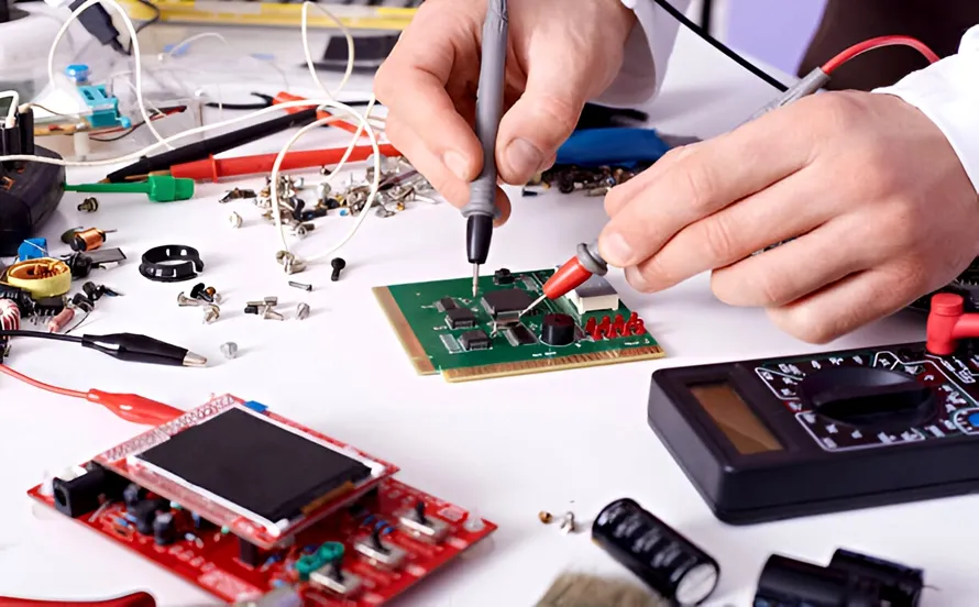
Introduction
In high-speed circuits, the physical dimensions of a printed circuit board play a critical role in maintaining signal integrity. Larger PCB sizes often lead to longer trace lengths, which exacerbate signal delays and increase the risk of reflections. Engineers designing high-frequency PCB layouts must balance compactness with functional requirements to optimize performance. This article explores how PCB size influences high-speed signal behavior, focusing on strategies for impedance matching and delay minimization. By understanding these relationships, designers can create more reliable circuits that meet stringent timing constraints. Proper high-frequency PCB design ensures data rates remain stable even as frequencies climb into the GHz range.
Why PCB Size Matters in High-Speed Circuits
PCB size directly affects the propagation paths for electrical signals in high-speed applications. As board dimensions increase, traces between components inevitably lengthen, amplifying propagation delays proportional to the distance traveled. In high-frequency PCB design, these delays can cause timing skew across differential pairs or clock signals, leading to setup and hold violations. Reflections arise when signals encounter impedance discontinuities along extended paths, such as unmatched vias or bends. Compact PCB sizes reduce these path lengths, inherently lowering both delays and reflection risks. Industry standards like IPC-2221 provide guidelines for routing and spacing that support signal integrity in such constrained environments.
Engineers often face trade-offs when minimizing PCB size, including component placement density and thermal management. Oversized boards may simplify initial layouts but introduce unnecessary signal degradation over time. Smaller boards demand precise planning to avoid crosstalk between closely spaced traces. Signal delays become more pronounced in larger formats because the signal's rise time approaches the propagation time, turning traces into transmission lines. Reflections compound this by creating ringing that distorts eye diagrams. Optimizing PCB size for high-speed circuits thus becomes a foundational step in achieving robust signal integrity.
Understanding Signal Delays in High-Speed PCBs
Signal delays in PCBs stem from the finite speed of electromagnetic wave propagation through the board's dielectrics. Every trace acts as a transmission line where delay scales linearly with length, making PCB size a primary determinant. In high-speed circuits, even modest increases in board dimensions can shift critical timing budgets, especially for synchronized signals like DDR memory interfaces. Designers must account for both intra-pair and inter-pair skew, which worsens with elongated routes. High-frequency PCB design mitigates this by prioritizing shortest paths during placement. Propagation velocity depends on the substrate's effective dielectric constant, but length remains the controllable factor tied to PCB size.
Minimizing PCB size reduces absolute delay without altering material properties. Longer traces not only delay signals but also attenuate them through resistive and dielectric losses, further degrading high-speed performance. In multi-layer stacks, vertical vias add microsecond-scale delays if not stub-minimized. Engineers simulate these effects early, but physical size dictates the baseline. Compact designs keep delays below rise time thresholds, preventing transmission line effects from dominating. This approach aligns with performance specifications outlined in IPC-6012E for rigid printed boards.
Delays manifest in real-world issues like bit errors or jitter in serial links. Oversized PCBs amplify intra-board skew, complicating clock distribution networks. By constraining size, teams enforce disciplined routing that equalizes path lengths. Feedback from prototypes often reveals delay hotspots linked to peripheral routing. Systematic size reduction streamlines these corrections. Ultimately, smaller PCBs enable tighter timing margins essential for multi-Gbps data rates.
Causes and Effects of Signal Reflections
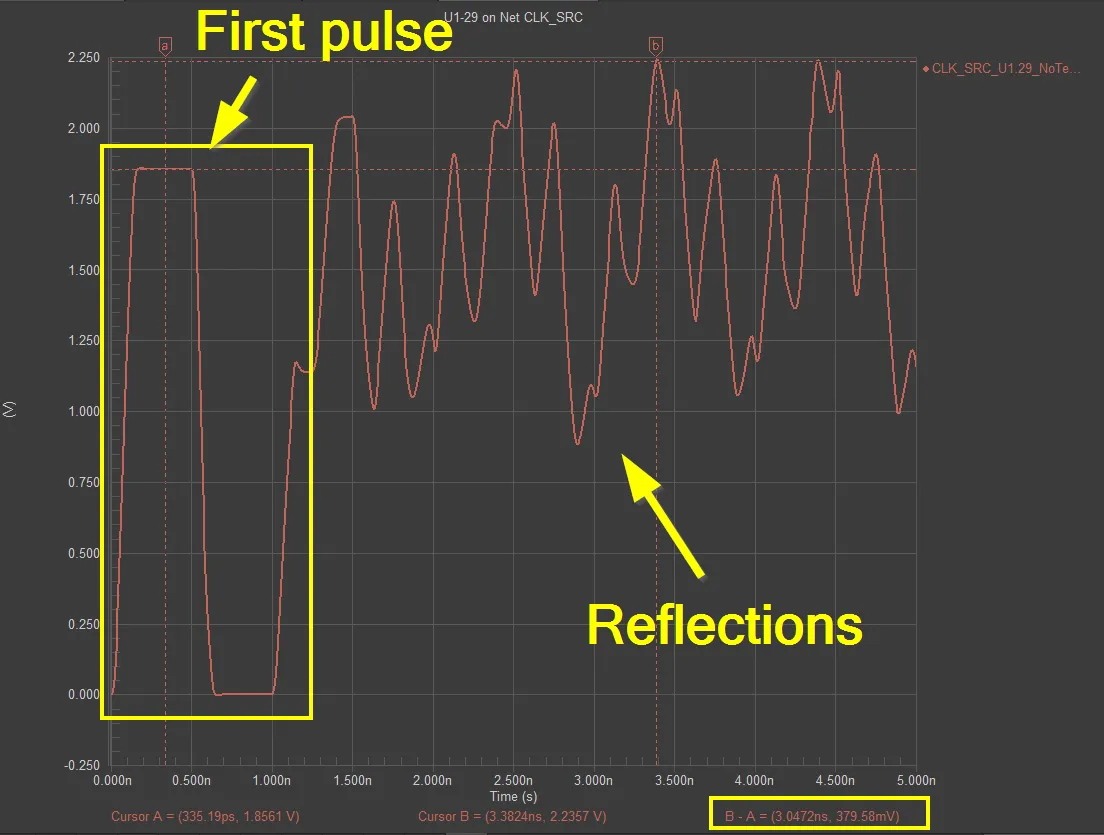
Signal reflections occur when a propagating wave encounters an impedance mismatch, partially bouncing back toward the source. In larger PCBs, extended traces heighten exposure to such discontinuities, including connector transitions, unterminated ends, or via stubs. These reflections superimpose on the original signal, causing overshoot, undershoot, and ringing that erode margins. High-speed circuits amplify this because wavelengths shorten, making even short mismatches significant. PCB size influences reflection magnitude by increasing the opportunity for cumulative errors along paths. Impedance matching becomes paramount to absorb energy and prevent echoes.
Common reflection sources include trace width variations, layer transitions, and bends exceeding radius guidelines. Larger boards necessitate more routing layers, multiplying via encounters and potential stubs. Reflections degrade eye opening, raising bit error rates in high-frequency applications. Engineers quantify this via time-domain reflectometry during validation. Compact PCB sizes limit routing complexity, reducing mismatch sites. Proper characteristic impedance control, around 50 or 100 ohms for singles or diffs, suppresses reflections effectively.
The interplay of size and reflections affects return loss and insertion loss metrics. Extended paths in big boards foster multi-reflection events that simulations must predict. Minimizing size shortens the reflection window, allowing faster settling times. Discontinuities like pads or splits act as stubs proportional to board scale. High-frequency PCB design employs stitching vias and ground planes to reference signals tightly. This structured mitigation preserves waveform fidelity across the link budget.
High-Frequency PCB Design Principles for Size Optimization
High-frequency PCB design prioritizes controlled impedance to counter size-induced issues. Characteristic impedance derives from trace geometry, stackup, and materials, remaining constant only with disciplined sizing. Engineers target uniform Z0 by modeling microstrip or stripline configurations early. PCB size constraints force hierarchical placement, grouping high-speed nets centrally. This reduces average trace lengths, inherently aiding impedance matching. Deviations from nominal Z0, even minor, provoke reflections scaled by path extent.
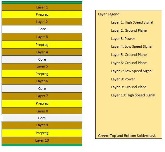
Layer stackup profoundly interacts with board size. Thinner boards suit compact designs but demand finer lines for impedance. Multi-layer configurations provide return paths close to signals, minimizing loop inductance regardless of size. However, larger PCBs strain plane splits, creating slit-induced reflections. Designers partition boards modularly if absolute minimization proves impractical. Adherence to standards like IPC-2141 for controlled impedance guides these choices across scales.
Dielectric choices influence velocity and loss, but size dictates raw delay. Low-loss materials help long paths, yet compact layouts obviate the need. Vias, inevitable in dense small boards, require back-drilling or blind types to eliminate stubs. Signal reflections from vias scale with board periphery. Optimization algorithms in layout tools enforce length rules tied to size budgets. This logical progression ensures delays stay predictable.
Best Practices for Minimizing Delays and Reflections
Start with component placement to minimize net lengths, centralizing high-speed devices on smaller PCBs. Group drivers, receivers, and clocks to enforce shortest routes. Avoid peripheral high-speed signals that elongate with board growth. Iterative floorplanning refines this, targeting under 10 cm paths for GHz signals where feasible. Impedance matching follows via stackup calculators ensuring consistent Z0. Termination resistors at ends absorb reflections, size-independent but path-critical.
Employ differential routing for balanced pairs, length-matching within tolerances. Ground planes under traces provide low-impedance returns, curbing EMI and reflections. Minimize vias through direct layer routing; use blind/buried where needed. Serpentine tuning equalizes longer paths without excessive size hikes. Pre-layout simulations predict delays using S-parameters. Post-route verification confirms impedance via TDR.
Fabrication tolerances impact high-speed performance, so specify tight controls per IPC-A-600K acceptability criteria. Panelization aids small prototypes, scaling to production. Thermal vias and copper pours manage heat in dense small boards. Crosstalk mitigation via spacing rules complements size reduction. These practices collectively tame signal delays and reflections.
For troubleshooting, inspect eye diagrams for closure indicating delays or ringing from reflections. Lengthy traces correlate with skew; compact redesign resolves. Mismatched Z0 shows as pre-shoot; recalculate geometries. Prototype testing with VNA quantifies issues tied to size.
Conclusion
Optimizing PCB size for high-speed circuits fundamentally reduces signal delays and reflections by shortening propagation paths. High-frequency PCB design thrives on compact layouts, precise impedance matching, and layered best practices. Engineers achieve this through structured placement, controlled stackups, and verification aligned with industry standards. Balancing size with functionality yields superior signal integrity, enabling reliable high-data-rate systems. Prioritizing these elements ensures circuits perform under demanding conditions. Future designs will lean further into miniaturization as speeds escalate.
FAQs
Q1: What is the ideal PCB size for high-speed circuits to minimize signal delays?
A1: Compact PCB sizes, often under standard panel fractions, best minimize signal delays by reducing trace lengths. Prioritize central placement of critical components to keep paths short. Combine with length matching for pairs. This approach lowers propagation times inherently. Impedance matching further stabilizes timing. High-frequency PCB design benefits most from such constrained footprints.
Q2: How does PCB size contribute to signal reflections in high-speed designs?
A2: Larger PCB sizes extend traces, increasing encounters with impedance discontinuities like vias and bends that cause reflections. Compact sizes limit these sites, preserving waveform integrity. Ensure uniform Z0 across paths. Ground referencing suppresses return path variations. Engineers model reflections early to size boards appropriately. Signal reflections diminish proportionally with reduced dimensions.
Q3: Why is impedance matching crucial in PCB size for high-speed circuits?
A3: Impedance matching prevents reflections by matching trace Z0 to source and load, regardless of size. In larger PCBs, mismatches amplify over length; smaller ones tolerate minor variances better. Control via geometry and stackup. Termination aids absorption. Simulations verify pre-fabrication. This practice underpins reliable high-frequency PCB design.
Q4: What best practices address signal delays from oversized PCBs?
A4: Minimize board size through efficient placement and multi-layer routing to shorten traces. Use differential pairs with length tuning. Solid ground planes reduce inductance. Avoid unnecessary vias. Prototype and measure delays. These steps optimize high-speed performance effectively.
References
IPC-2221B — Generic Standard on Printed Board Design. IPC, 2012
IPC-6012E — Qualification and Performance Specification for Rigid Printed Boards. IPC, 2015
IPC-2141A — Design Guide for High-Speed Controlled Impedance Circuit Boards. IPC, 2009
IPC-A-600K — Acceptability of Printed Boards. IPC, 2020