Introduction
Printed Circuit Board (PCB) stackup design plays a pivotal role in ensuring signal integrity and smooth operation in modern electronic systems. As circuits become faster and more complex, maintaining controlled impedance becomes essential to prevent signal degradation. The arrangement of layers, dielectric materials, and trace geometries directly influences how signals propagate through the board. For electrical engineers, understanding the relationship between PCB stackup and impedance control is critical to designing reliable, high performance circuits. This article explores the technical aspects of stackup design, its impact on impedance, and best practices for optimizing signal integrity. By focusing on layer arrangement and adjacent traces, engineers can mitigate issues like crosstalk and ensure consistent performance in high speed applications.
What Is PCB Stackup and Why It Matters
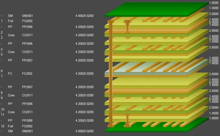
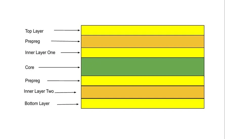
PCB stackup refers to the arrangement of conductive and insulating layers within a printed circuit board. These layers include signal planes, ground planes, power planes, and dielectric materials that separate them. The stackup configuration determines how electrical signals travel through the board and interact with each other. For electrical engineers, a well planned stackup is vital because it affects impedance control, signal integrity, and overall circuit performance.
Impedance control is the practice of maintaining a consistent characteristic impedance along signal traces to ensure signals are transmitted without distortion. Mismatches in impedance can lead to reflections, signal loss, or timing issues, especially in high speed digital and RF applications. A poorly designed stackup can disrupt smooth operation by introducing noise or crosstalk between adjacent traces. Therefore, stackup design is not just a structural choice but a fundamental aspect of achieving reliable electrical performance. Standards like IPC-6012E provide guidelines for stackup configurations to meet performance specifications.
Technical Principles of PCB Stackup and Impedance Control
Impedance in a PCB is determined by the trace width, thickness, dielectric constant of the insulating material, and the distance between the trace and reference planes. The stackup configuration directly influences these parameters. For instance, placing a signal layer between two ground planes creates a controlled environment for signal propagation, reducing electromagnetic interference (EMI) and crosstalk.
In high speed designs, signal integrity relies on maintaining a consistent impedance value, often 50 ohms for RF circuits or 100 ohms for differential pairs. If the stackup places signal traces too close to each other or without proper grounding, impedance mismatches occur. This can cause signal reflections, where part of the signal bounces back, degrading performance. The dielectric thickness between layers also plays a role, as it affects the capacitance and thus the impedance of the trace.
Adjacent traces on the same layer or across layers can couple, leading to crosstalk, which further compromises signal integrity. A balanced stackup minimizes this by ensuring adequate spacing and using ground planes as shields. Engineers must calculate impedance based on stackup parameters using established formulas or tools for signal integrity analysis. These tools help predict how layer arrangements impact trace behavior and allow for adjustments before fabrication.
Related Reading: Power and Ground Plane Design in 4 Layer PCBs
Impact of Stackup on Signal Integrity and Smooth Operation
Signal integrity encompasses the quality of electrical signals as they travel through the PCB. A well designed stackup preserves signal integrity by minimizing noise, reflections, and crosstalk. For example, placing high speed signal layers adjacent to ground planes provides a low impedance return path for currents, reducing loop inductance. This setup is crucial for smooth operation in applications like data communication or microprocessors.
Conversely, an unbalanced stackup, such as placing signal layers too far from reference planes, increases loop areas and inductance, leading to EMI issues. Crosstalk between adjacent traces becomes more pronounced if spacing is insufficient or if no shielding layers are present. In multilayer boards, engineers often alternate signal and ground layers to create a controlled impedance environment and isolate sensitive signals.
Material selection also ties into stackup design. Dielectric materials with stable constants ensure consistent impedance across frequencies. Variations in material properties can disrupt signal integrity, especially in high frequency designs. Following guidelines from standards like IPC-A-600K ensures that stackup configurations meet acceptability criteria for performance and manufacturability.
Related Reading: PCB Grounding Techniques: A Guide to Minimizing Noise and Ensuring Reliable Connections
Practical Solutions for Optimizing Stackup in Impedance Control
Designing a PCB stackup for impedance control requires careful planning and adherence to best practices. Below are actionable steps electrical engineers can follow to achieve optimal results.
- Layer Arrangement: Position high speed signal layers next to ground planes to create a controlled impedance path. For a four layer board, a common stackup is signal, ground, power, and signal. This isolates signals and minimizes interference.
- Dielectric Thickness: Select dielectric materials with known constants and consistent thickness. Thinner dielectrics reduce loop inductance but may increase capacitance, so balance is key.
- Trace Spacing: Maintain adequate spacing between adjacent traces to prevent crosstalk. Standards like IPC-6012E provide recommendations for minimum spacing based on signal type and board class.
- Ground Planes: Use continuous ground planes beneath signal layers to provide a return path and shield against EMI. Avoid splitting ground planes under high speed traces.
- Simulation Tools: Utilize tools for signal integrity analysis to model stackup configurations. These tools calculate impedance based on layer stackup and trace geometry, allowing for design adjustments before manufacturing.
Symmetry in stackup design also helps prevent mechanical stress during fabrication, which can affect electrical performance. A balanced stackup reduces the risk of warpage, ensuring traces remain aligned with calculated impedance values.
Best Practices for Managing Adjacent Traces in Stackup Design
Adjacent traces pose a significant challenge in maintaining signal integrity, especially in dense PCB layouts. When traces run parallel for long distances, they can couple, leading to crosstalk. Stackup design offers solutions to mitigate this issue.
First, ensure that high speed traces on the same layer are spaced adequately apart. If space constraints prevent this, route critical signals on different layers, separated by ground or power planes. Vertical separation is often more effective than horizontal spacing in reducing interference. Second, maintain consistent trace widths to avoid impedance discontinuities, which can exacerbate crosstalk effects.
In multilayer boards, dedicate specific layers to sensitive signals and surround them with reference planes. This configuration acts as a shield, isolating signals from adjacent traces. Engineers should also avoid routing high speed signals over splits in ground planes, as this disrupts return paths and increases noise.
Troubleshooting Stackup Related Impedance Issues
When impedance control fails due to stackup design, engineers must systematically identify and resolve the issue. Start by reviewing the layer arrangement against design specifications. If signal layers are not adjacent to reference planes, consider revising the stackup to include additional ground layers.
Next, measure trace impedance using time domain reflectometry to identify mismatches. If discrepancies exist, adjust trace widths or dielectric thickness to align with target values. Simulation tools for signal integrity can predict how changes in stackup affect performance, reducing trial and error.
Material inconsistencies can also cause impedance variations. Verify that dielectric properties match design requirements, referring to standards like IPC-A-600K for acceptable tolerances. Finally, inspect the board for manufacturing defects, such as uneven layer bonding, which can alter impedance characteristics.
Conclusion
PCB stackup design is a cornerstone of impedance control and signal integrity in modern electronics. By carefully arranging layers, selecting appropriate materials, and managing adjacent traces, electrical engineers can ensure smooth operation in high speed and high frequency applications. A well planned stackup minimizes signal degradation, reduces crosstalk, and maintains consistent impedance, all of which are essential for reliable circuit performance. Adhering to industry standards and using tools for signal integrity analysis further enhances design accuracy. As circuit complexity continues to grow, mastering stackup design remains a critical skill for achieving optimal electrical performance.
FAQs
Q1: How does PCB stackup influence signal integrity in high speed designs?
A1: PCB stackup directly impacts signal integrity by determining impedance and return paths. A balanced stackup with signal layers near ground planes reduces noise and reflections. Proper layer arrangement minimizes crosstalk between adjacent traces, ensuring clean signal transmission. Following industry standards helps maintain consistent performance in high speed applications.
Q2: What role do tools for signal integrity play in stackup design?
A2: Tools for signal integrity analyze how stackup configurations affect impedance and signal behavior. They simulate trace performance, predict reflections, and identify crosstalk risks. By modeling different layer arrangements, engineers can optimize stackup for smooth operation before fabrication, saving time and reducing errors.
Q3: Why is spacing between adjacent traces important in stackup planning?
A3: Spacing between adjacent traces prevents crosstalk, which degrades signal integrity. Inadequate spacing causes electromagnetic coupling, especially in high speed circuits. Stackup design can isolate traces using ground planes, while proper spacing on the same layer further reduces interference, ensuring reliable signal transmission.
Q4: How can stackup design ensure smooth operation in multilayer PCBs?
A4: Stackup design ensures smooth operation by aligning signal layers with reference planes to control impedance. It minimizes EMI and crosstalk through strategic layer placement. Selecting stable dielectric materials and maintaining symmetry also prevents mechanical issues, supporting consistent electrical performance in multilayer boards.
References
IPC-6012E - Qualification and Performance Specification for Rigid Printed Boards. IPC, 2020.
IPC-A-600K - Acceptability of Printed Boards. IPC, 2020.


