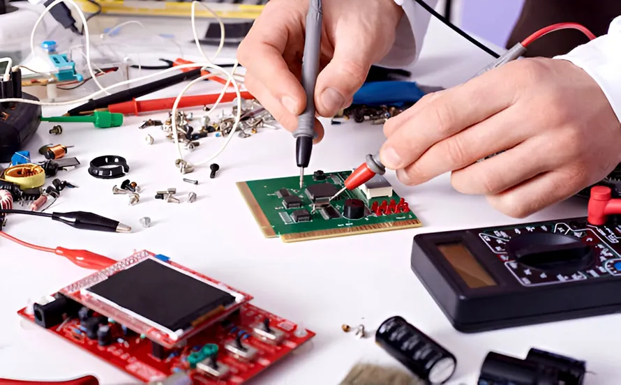
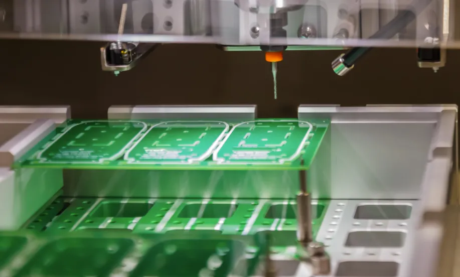
Introduction
Printed circuit boards form the backbone of electronic assemblies, yet achieving and maintaining flatness remains a persistent challenge in manufacturing. PCB warpage and twist, often referred to collectively as bow and twist, represent common PCB manufacturing defects that compromise reliability and assembly yields. These deformations occur when boards deviate from their intended planar shape, leading to issues during surface mount technology processes and long-term performance. Electrical engineers must understand these phenomena to design robust boards and collaborate effectively with fabricators. This article delves into the root causes of PCB warpage and twist, explores measurement techniques aligned with industry standards, and outlines practical strategies for ensuring PCB flatness. By addressing these factors systematically, teams can produce reliable boards that meet stringent quality requirements.
What Is PCB Warpage and Twist? Why It Matters
PCB warpage manifests as an overall bending of the board out of its plane, while twist involves a rotational deformation where opposite corners lift differently relative to the board's edges. Bow represents a cylindrical curvature along the length or width, and twist creates a parallelogram-like distortion diagonally. These PCB manufacturing defects directly impact assembly processes, as even minor deviations can misalign components during reflow soldering or cause bridging in fine-pitch devices. In high-density interconnect boards, poor PCB flatness exacerbates stencil printing inconsistencies and pick-and-place errors, reducing first-pass yields. Beyond assembly, warpage induces mechanical stresses on solder joints, accelerating fatigue and failure in operational environments. Standards like IPC-6012 define acceptable limits for bow and twist to ensure boards perform reliably in demanding applications.
Maintaining PCB flatness is critical for electrical engineers working on multilayer designs, where thermal cycling amplifies deformation risks. Excessive bow and twist can lead to signal integrity issues from uneven dielectric spacing or impedance variations. In automotive or aerospace sectors, these defects compromise structural integrity under vibration and temperature extremes. Fabricators inspect panels against IPC-A-600 criteria to classify acceptability, emphasizing the need for proactive design and process controls. Ultimately, minimizing PCB warpage and twist enhances product lifespan, cuts rework costs, and supports scalable production.
Technical Causes of PCB Warpage and Twist
Uneven copper distribution across layers stands as a primary driver of PCB warpage during fabrication. When copper planes differ significantly in area or thickness between top and bottom sides, thermal expansion mismatches generate residual stresses post-etching. Lamination processes exacerbate this, as heat and pressure cause prepreg materials to flow asymmetrically around unbalanced copper features. Thin boards or large panels amplify the effect, as rigidity decreases with reduced thickness. Hygroscopic moisture absorption further contributes, swelling resins unevenly and promoting twist upon heating.
Material selection plays a pivotal role in bow and twist susceptibility. Coefficient of thermal expansion differences between copper foil, laminate cores, and prepregs induce warping during press cycles, where temperatures exceed glass transition points. Low-Tg materials deform more readily under reflow profiles, locking in permanent bends. Mixed resin systems or inconsistent prepreg thickness compound these issues, creating internal gradients. Board geometry influences outcomes too; long, narrow panels twist easily due to edge effects during handling and cooling.
Manufacturing processes introduce additional vectors for PCB manufacturing defects. Rapid cooling after hot air solder leveling or plating shocks the board, inducing twist from differential contraction rates. Improper panel routing leaves unsupported edges that bow under gravity. Over-etching thins copper unevenly, while drill smear residue affects layer bonding integrity. Cumulative effects from multiple cycles, including multilayer pressing and surface finishes, demand vigilant process monitoring to preserve PCB flatness.
Environmental factors like storage humidity also trigger latent warpage. Absorbed moisture expands during preheating, bowing panels before assembly. Vibration during shipping or handling fatigues weak points, manifesting as twist. These extrinsic causes interact with intrinsic design flaws, underscoring the need for holistic mitigation.
Measurement Methods for PCB Flatness
Accurate assessment of PCB warpage relies on standardized techniques outlined in IPC-TM-650 method 2.4.22. Engineers place the board on a flat granite surface, ensuring no air gaps, and measure deviations at multiple points using a dial indicator or laser profiler. For bow, probes capture height differences along the longest dimension; twist calculations involve diagonal corner lifts relative to the board's diagonal length. Panels exceeding specified percentages prompt rejection or rework.
Advanced tools like shadow moiré interferometry provide dynamic flatness data at elevated temperatures, simulating reflow conditions. This reveals transient warpage peaks critical for BGA assemblies. Electrical engineers benefit from these metrics to validate designs pre-production. Consistent measurement across lots ensures traceability and process stability.
Implementing Strategies for Flat and Reliable Boards
Design practices form the first line of defense against PCB warpage. Engineers should symmetrize stackups by mirroring copper weights and plane areas across the neutral axis, minimizing expansion differentials. For multilayer boards, route high-current traces evenly and fill unused areas with balanced pours. Select high-Tg laminates to withstand thermal excursions without softening. Smaller panel sizes or router tabs enhance rigidity during handling.
Manufacturing optimizations target process-induced stresses. Fabricators apply controlled press cycles with gradual ramps and dwells, followed by slow cooling under pressure to equalize contractions. Pre-baking panels removes moisture, preventing popcorn effects. Symmetric routing sequences and fixture-supported etching maintain planarity. For thick copper builds, sequential lamination reduces cumulative warpage.
Assembly-stage interventions further safeguard PCB flatness. Bake boards prior to reflow to desorb humidity, and use nitrogen atmospheres to curb oxidation-related bowing. Fixtures or carriers constrain panels during soldering, countering thermal ramps. Post-reflow inspections flag outliers for flattening via heat/pressure treatments.
Material and tooling synergies yield superior results. Matching CTE values across core, prepreg, and foil prevents delamination-driven twist. High-modulus resins add stiffness to thin boards. Vacuum-assisted lamination expels voids, ensuring uniform flow. Collaborative DFM reviews between design and fab teams preempt defects.
Troubleshooting Common Bow and Twist Scenarios
When warpage appears post-lamination, audit copper balance ratios; deviations over 15% often correlate with bow. Twist in routed panels signals asymmetric drilling or V-scoring. Reflow-induced defects trace to moisture or asymmetric component loading. Iterative shadow moiré testing pinpoints temperature hotspots. Corrective presses with fixtures recover many boards within tolerance.
Conclusion
PCB warpage and twist demand attention across the product lifecycle to deliver flat, reliable boards. By understanding causes from material mismatches to process shocks, electrical engineers can implement targeted designs like symmetric stackups and high-Tg selections. Manufacturing best practices, including controlled thermal profiles and precise measurements per IPC standards, minimize defects. Proactive collaboration ensures PCB flatness meets application needs, boosting yields and longevity. Adopting these strategies transforms potential PCB manufacturing defects into controlled variables, fostering high-performance electronics.
FAQs
Q1: What are the main causes of PCB warpage during manufacturing?
A1: Uneven copper distribution, thermal expansion mismatches in stackups, and rapid cooling after processes like lamination or plating primarily cause PCB warpage. Moisture absorption swells resins asymmetrically upon heating. Board geometry, such as large thin panels, amplifies these effects. Addressing copper balance and process controls early prevents most instances.
Q2: How does IPC-6012 address PCB twist tolerances?
A2: IPC-6012 specifies qualification criteria for rigid boards, including maximum allowable bow and twist based on class and surface mount usage. It guides fabricators on flatness requirements to ensure assembly compatibility. Engineers reference it during design reviews to align with production capabilities. Compliance verifies reliability under thermal stress.
Q3: What design strategies improve PCB flatness?
A3: Symmetrize copper layers and planes across the stackup to counter expansion forces. Choose materials with matched CTE and high Tg for thermal stability. Minimize board aspect ratios and add fill patterns for even mass distribution. These steps reduce PCB warpage risks from the outset.
Q4: How can PCB warpage be measured accurately?
A4: Use IPC-TM-650 2.4.22 by placing the board on a flat surface and probing deviations with dial gauges along edges and diagonals. Shadow moiré captures dynamic warpage at reflow temperatures. Regular checks ensure panels meet flatness specs before assembly.
References
IPC-6012E — Qualification and Performance Specification for Rigid Printed Boards. IPC, 2017
IPC-A-600K — Acceptability of Printed Boards. IPC, 2020
IPC-TM-650 2.4.22 — Bow and Twist. IPC, 2022