Introduction
Polyimide PCBs represent a cornerstone in flexible electronics, offering exceptional thermal stability and mechanical flexibility for demanding applications. These boards, built on polyimide substrates, excel in environments where standard materials falter under heat stress. However, as power densities rise in compact devices, effective heat management becomes critical to prevent performance degradation and failure. Polyimide PCB thermal vias emerge as a key solution, channeling heat away from critical components through the board's layers. This approach enhances via heat dissipation while preserving the inherent bendability of flexible designs. Engineers must understand thermal via design to optimize flexible PCB thermal management.
What Are Polyimide PCB Thermal Vias and Why Do They Matter?
Polyimide PCB thermal vias are plated through-holes specifically engineered to conduct heat vertically across the flexible board structure. Unlike standard signal vias, these prioritize thermal conductivity, leveraging copper plating to transfer heat from surface-mounted components to internal planes or the opposite side. In polyimide substrates, known for their high thermal endurance, thermal vias bridge the gap between the material's low inherent conductivity and the need for efficient dissipation. They matter because flexible PCBs often house power-hungry elements in confined spaces, such as sensors or LEDs in wearables, where heat buildup can cause delamination or trace cracking.
The relevance intensifies in dynamic applications requiring repeated flexing, where poor thermal management accelerates fatigue. According to IPC-6013, qualification for flexible boards emphasizes thermal shock resistance, underscoring the role of vias in maintaining integrity. Without proper via heat dissipation, hotspots form, elevating junction temperatures and shortening component life. Thus, integrating polyimide PCB thermal vias ensures reliability in high-reliability sectors.
Technical Principles of Via Heat Dissipation in Flexible Designs
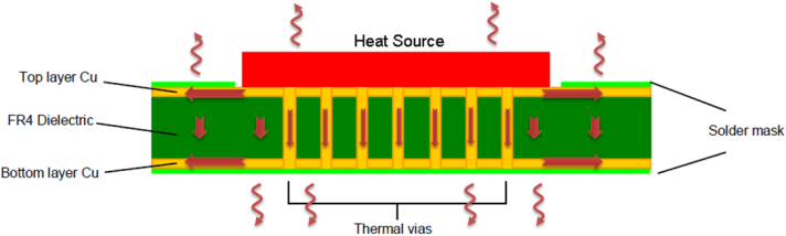
Heat dissipation via thermal vias relies on conduction through the copper barrel, which boasts far superior thermal conductivity compared to polyimide dielectrics. When placed under a heat source, the via captures localized heat and funnels it to copper planes that spread it laterally, minimizing gradients. In multilayer flexible stacks, multiple vias form arrays, multiplying pathways and reducing thermal resistance. This mechanism proves vital in polyimide PCBs, where the substrate's stability supports aggressive thermal cycling without warping.
Convection and radiation play secondary roles, but conduction dominates in compact flex designs. Engineers model this using Fourier's law, where heat flux depends on the temperature differential and material properties. Polyimide's low thermal expansion coefficient aids compatibility, preventing stress at via interfaces during temperature swings. Overall, these principles enable flexible PCB thermal management without compromising bend radius.
Thermal Via Design Considerations for Polyimide Substrates
Effective thermal via design starts with selecting appropriate plating thickness to maximize conductivity while adhering to fabrication limits. Filled vias, incorporating conductive epoxy or copper plugs, offer enhanced performance by eliminating air gaps and providing mechanical reinforcement in flex environments. Tenting the vias with solder mask protects against contamination but requires high-conductivity fills to avoid impeding heat flow. In polyimide constructions, designers prioritize blind or buried vias where possible to shorten paths and boost efficiency.
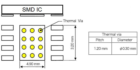
Aspect ratio control ensures uniform plating, critical for reliability under flex stress. Arrays optimize coverage under thermal pads, balancing density with routing space. IPC-2221 provides generic guidelines for such designs, stressing connections to dedicated planes. Compatibility with polyimide's properties demands attention to CTE matching, averting cracks during assembly reflow.
Best Practices for Thermal Via Placement in Flexible Designs
Strategic thermal via placement centers on positioning arrays directly beneath component thermal pads, maximizing direct heat capture. Space vias to prevent solder wicking during assembly, ensuring reliable joints without bridging. In flexible regions, confine placements to rigid or static zones, as per IPC-2223 recommendations, to dodge fatigue from bending. Factory insights reveal that offsetting vias slightly from pad edges reduces stress concentrations, enhancing longevity.
Integrate vias with ground planes via stitched connections for lateral spreading. For high-power spots, scale array size proportionally to dissipation needs, verified through simulation. Collaborate with fabricators early to align on drill and fill processes suited to polyimide stacks. These practices elevate via heat dissipation in demanding flexible PCB thermal management scenarios.
Challenges in Flexible PCB Thermal Management and Solutions
Flexible designs face unique hurdles in thermal management due to thin profiles limiting plane areas and bending inducing via stress. Polyimide mitigates substrate degradation but cannot fully compensate for clustered hotspots. Vias in dynamic flex zones risk cracking, prompting relocation to stiffener-supported areas. Solutions include filled vias for robustness and cross-hatched planes for balanced flex and conduction.
Moisture absorption, though low in polyimide, affects plating adhesion post-bake, necessitating controlled storage. Thermal simulation tools predict flows, guiding iterative placement. Layer sequencing places power planes near components for shorter paths. These targeted approaches resolve issues, aligning with standard qualification per IPC-6013.
Another challenge arises from assembly, where reflow profiles strain vias. Pre-tinning or selective soldering preserves integrity. Hybrid rigid-flex transitions demand careful via fencing to isolate thermal zones. Factory-driven validation through thermal cycling confirms robustness.
Advanced Insights: Optimizing for High-Density Applications
In high-density polyimide PCBs, microvia integration refines thermal via design, enabling tighter arrays without sacrificing signal integrity. Staggered patterns distribute load evenly, curbing electromagnetic interference. Polyimide's chemical resistance supports aggressive plating chemistries for thicker copper. Engineers leverage symmetric stackups to neutralize bend-induced warping around vias.
Troubleshooting hotspots involves infrared mapping post-prototype, refining placement iteratively. Ground via stitching complements thermal arrays, forming a robust dissipation network. These insights, rooted in manufacturing realities, empower precise flexible PCB thermal management.
Conclusion
Polyimide PCB thermal vias stand as indispensable for superior via heat dissipation in flexible designs, harnessing conduction to safeguard performance. Thoughtful thermal via design, placement, and integration with planes address heat challenges inherent to flex substrates. Adhering to standards like IPC-2221 and IPC-6013 ensures qualification and reliability. Engineers achieve optimal thermal via placement by prioritizing static zones and simulation-driven arrays. Ultimately, these strategies extend device lifespans, enabling innovation in compact, high-power electronics.
FAQs
Q1: What role do polyimide PCB thermal vias play in flexible PCB thermal management?
A1: Polyimide PCB thermal vias conduct heat vertically from components to internal planes, preventing hotspots in flexible designs. They leverage copper's conductivity against polyimide's lower baseline, essential for high-power flex circuits. Best practices include arrays under pads and filled structures for durability. This enhances overall reliability without rigidifying the board.
Q2: How does thermal via placement affect via heat dissipation in polyimide flex PCBs?
A2: Thermal via placement directly under thermal pads maximizes heat capture, with arrays spreading load effectively. Avoid bend areas to prevent cracking, aligning with IPC-2223. Factory spacing prevents wicking, optimizing flow to planes. Simulation refines density for specific dissipation needs. Proper placement boosts efficiency by reducing thermal resistance significantly.
Q3: What are key considerations in thermal via design for flexible PCBs?
A3: Thermal via design in flexible PCBs emphasizes filled or blind types for strength in polyimide stacks. Control aspect ratios for plating uniformity and connect to ground planes. CTE matching averts stress during cycling. IPC-6013 guides qualification. These ensure robust via heat dissipation amid flex demands.
Q4: Why avoid thermal vias in dynamic flex zones of polyimide PCBs?
A4: Dynamic flex zones stress vias, risking plating cracks and failures under repeated bending. IPC-2223 advises static area placement. Use stiffeners for support if needed. Alternatives like edge planes maintain thermal management. This preserves flexible PCB thermal management integrity long-term.
References
IPC-6013DS — Qualification and Performance Specification for Flexible and Rigid-Flex Printed Boards. IPC, 2014
IPC-2221F — Generic Standard on Printed Board Design. IPC, 2020
IPC-2223C — Sectional Design Standard for Flexible/Rigid-Flexible Printed Boards. IPC, 2019


