Introduction
In the realm of printed circuit board design, 4-layer PCBs stand as a cornerstone for many electronic applications, offering a balance between complexity and cost. A critical aspect of their design lies in the effective implementation of power and ground planes. These planes are essential for maintaining power integrity, reducing noise, and ensuring stable operation of electronic circuits. For electrical engineers, understanding the nuances of 4-layer PCB power plane and ground plane design is vital to achieving optimal performance in modern devices. This article delves into the principles and best practices of 4-layer PCB PDN design, focusing on noise reduction and power integrity. By exploring technical foundations and practical strategies, engineers can enhance their designs to meet stringent performance requirements in high-speed and power-sensitive applications.
What Are Power and Ground Planes in 4-Layer PCBs and Why Do They Matter
Power and ground planes in a 4 layers PCB are dedicated layers within the board's stackup that distribute power and provide a reference for electrical signals. Typically, a 4-layer PCB consists of two signal layers on the outer surfaces and two internal planes, often designated as power and ground. These planes serve as low-impedance paths for current, ensuring stable voltage delivery and minimizing electromagnetic interference. Their importance cannot be overstated, as they directly impact power integrity and noise levels in a circuit. Poorly designed planes can lead to voltage drops, crosstalk, and signal distortion, compromising device functionality. For engineers working on high-speed or mixed-signal designs, mastering 4-layer PCB power plane and ground plane layouts is crucial to achieving reliable performance and meeting industry standards like those set by IPC.
Technical Principles of Power and Ground Plane Design in 4-Layer PCBs
Stackup Configuration for Optimal Performance
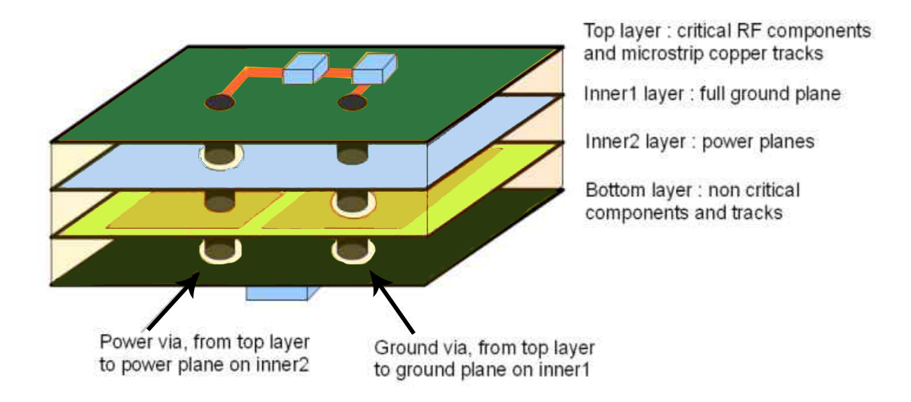
A standard 4-layer PCB stackup often follows a signal-ground-power-signal arrangement. The top and bottom layers handle signal traces, while the inner layers are dedicated to ground and power planes. This configuration ensures that signals are closely coupled to a reference plane, reducing loop inductance and improving noise reduction in 4-layer PCBs. The ground plane acts as a return path for signals, minimizing electromagnetic interference. Placing the ground plane adjacent to signal layers also helps in controlling impedance for high-speed traces. Engineers must ensure that the power plane is continuous and not fragmented excessively to maintain low impedance across the board. Following guidelines from standards such as IPC-2221B helps in defining appropriate layer spacing and dielectric thickness for optimal power integrity.
Power Distribution Network Design Considerations
The power distribution network, or PDN, in a 4-layer PCB is responsible for delivering stable voltage to all components. Effective 4-layer PCB PDN design requires minimizing voltage drops and ensuring low impedance across frequencies. This involves strategic placement of decoupling capacitors near power pins of integrated circuits to filter high-frequency noise. The power plane must be designed to handle the current demands of the circuit without significant voltage fluctuations. Engineers should calculate the required copper thickness based on current density, adhering to standards like IPC-2152 for thermal and electrical safety. Additionally, splitting the power plane into different voltage domains, if needed, must be done carefully to avoid coupling noise between domains, thus preserving 4-layer PCB power integrity.
Ground Plane Integrity and Noise Reduction
The ground plane in a 4-layer PCB serves as a common reference for all signals and a return path for currents. A solid, unbroken ground plane is essential for 4-layer PCB noise reduction, as it minimizes loop areas that can induce electromagnetic interference. Slots or cuts in the ground plane should be avoided beneath high-speed signal traces to prevent return path discontinuities. Multiple vias connecting ground planes across layers can further reduce impedance and enhance shielding. Standards such as IPC-2221B provide guidance on via placement and ground plane design to ensure signal integrity. A well-designed ground plane also aids in dissipating heat, contributing to the overall stability of the circuit.
Best Practices for 4-Layer PCB Power and Ground Plane Design
Prioritize Continuous Planes for Low Impedance
To achieve optimal 4-layer PCB power integrity, both power and ground planes should be as continuous as possible. Breaks or splits in these planes increase impedance and can lead to noise coupling. If splitting the power plane for multiple voltage levels is necessary, ensure that each section is large enough to maintain low impedance. Ground planes should ideally remain unbroken, especially under high-speed signal traces. Using design rules from IPC-6012E ensures that plane integrity is maintained during fabrication, preventing manufacturing defects that could compromise performance.
Strategic Placement of Decoupling Capacitors
Decoupling capacitors play a critical role in 4-layer PCB noise reduction by filtering transient currents and stabilizing voltage levels. Place these capacitors as close as possible to the power pins of active components to minimize inductance. Use a range of capacitor values to cover different frequency bands, ensuring a robust PDN. Vias connecting capacitors to power and ground planes should be short and direct to reduce parasitic effects. Following recommendations from JEDEC J-STD-020E for component placement can help in achieving reliable soldering and electrical connections.
Minimize Crosstalk with Proper Layer Spacing
Crosstalk between signal traces can degrade performance in a 4-layer PCB. To mitigate this, ensure adequate spacing between signal layers and their adjacent reference planes. The dielectric thickness between layers, as specified in IPC-2221B, should be chosen to control impedance and reduce coupling. Routing high-speed signals on the top layer with a ground plane directly beneath minimizes interference. Avoid routing sensitive analog signals near noisy digital lines to preserve signal quality and enhance 4-layer PCB power integrity.
Related Reading: High Frequency PCB Routing Techniques: Minimizing Signal Loss and Interference
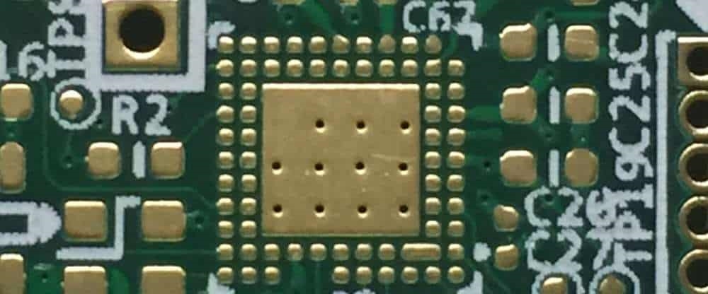
Use Vias Effectively for Plane Connections
Vias are essential for connecting components to power and ground planes in a 4-layer PCB. However, excessive vias can introduce inductance and disrupt plane continuity. Use multiple ground vias near high-current components to ensure low-impedance paths. Place vias strategically to avoid creating large current loops that can radiate noise. Standards like IPC-A-600K provide criteria for via quality and placement, ensuring reliability during manufacturing and operation.
Troubleshooting Common Issues in 4-Layer PCB PDN Design
Addressing Voltage Drops in Power Planes
Voltage drops in a 4-layer PCB power plane can lead to insufficient power delivery to components. This often results from inadequate copper thickness or excessive plane splits. Engineers should verify current requirements and ensure compliance with IPC-2152 for conductor sizing. Widening power traces or adding more vias to the power plane can help distribute current evenly. Simulation tools adhering to industry standards can predict potential drops before fabrication, allowing for design adjustments.
Reducing Electromagnetic Interference
Electromagnetic interference is a common challenge in 4-layer PCB designs, often caused by improper grounding or signal routing. Ensure that the ground plane is continuous and directly beneath signal layers to provide a low-impedance return path. Avoid routing signals over splits in ground or power planes. Adding ground pours in unused areas of signal layers can further shield against interference, enhancing 4-layer PCB noise reduction as per IPC-2221B guidelines.
Managing Thermal Stress on Planes
High current densities in power planes can generate heat, leading to thermal stress in a 4-layer PCB. Engineers must design planes with sufficient copper thickness to handle thermal loads, following IPC-2152 for current-carrying capacity. Thermal vias connecting to ground planes can aid in heat dissipation. Monitoring junction temperatures during testing ensures compliance with standards like JEDEC J-STD-020E, preventing long-term reliability issues.
Conclusion
Designing power and ground planes in 4-layer PCBs is a fundamental skill for electrical engineers aiming to ensure power integrity and noise reduction. By adhering to a well-thought-out stackup, prioritizing continuous planes, and strategically placing components like decoupling capacitors, engineers can achieve robust 4-layer PCB PDN design. Addressing common challenges such as voltage drops, electromagnetic interference, and thermal stress through best practices ensures reliable performance in demanding applications. Standards from IPC and JEDEC provide a solid foundation for creating designs that meet industry expectations. With careful planning and attention to detail, 4-layer PCB power plane and ground plane designs can significantly enhance the functionality and longevity of electronic systems.
FAQs
Q1: What is the ideal stackup for a 4-layer PCB power plane and ground plane design?
A1: The most common stackup for a 4-layer PCB is signal-ground-power-signal. This arrangement ensures signals are coupled to a reference plane, reducing noise and maintaining impedance control. The ground plane provides a return path, while the power plane delivers stable voltage. Following IPC-2221B guidelines for layer spacing ensures optimal performance and 4-layer PCB power integrity in high-speed and mixed-signal applications.
Q2: How can I achieve 4-layer PCB noise reduction through ground plane design?
A2: A solid, continuous ground plane is key to 4-layer PCB noise reduction. Avoid slots or cuts under high-speed traces to prevent return path disruptions. Use multiple ground vias near components to minimize impedance. Ensure the ground plane is adjacent to signal layers for better shielding, as recommended by IPC-2221B, to reduce electromagnetic interference and enhance overall circuit stability.
Q3: What are common mistakes in 4-layer PCB PDN design to avoid?
A3: Common mistakes in 4-layer PCB PDN design include excessive splits in power planes, leading to high impedance, and poor placement of decoupling capacitors, increasing noise. Ignoring via inductance or inadequate copper thickness for current loads can cause voltage drops. Adhering to IPC-2152 for conductor sizing and strategic component placement helps prevent these issues and ensures reliable performance.
Q4: How does capacitor placement affect 4-layer PCB power integrity?
A4: Capacitor placement is critical for 4-layer PCB power integrity. Decoupling capacitors should be placed near power pins of components to filter noise and stabilize voltage. Short, direct vias to power and ground planes reduce inductance. Using a range of capacitor values addresses various frequencies, ensuring a robust PDN as per JEDEC J-STD-020E guidelines for component reliability.
References
IPC-2221B — Generic Standard on Printed Board Design. IPC, 2012.
IPC-6012E — Qualification and Performance Specification for Rigid Printed Boards. IPC, 2020.
IPC-2152 — Standard for Determining Current Carrying Capacity in Printed Board Design. IPC, 2009.
IPC-A-600K — Acceptability of Printed Boards. IPC, 2020.
JEDEC J-STD-020E — Moisture/Reflow Sensitivity Classification for Nonhermetic Surface Mount Devices. JEDEC, 2014.


