Introduction
Engineers working on high-frequency circuits often rely on specialized laminates to maintain signal integrity across RF and microwave applications. Rogers PCBs, known for their low-loss properties and stable dielectric constants, demand precise impedance control to prevent signal reflections and distortions. A Rogers PCB impedance calculator serves as an essential tool for determining optimal trace geometries in these designs. This practical guide explains the fundamentals of PCB impedance matching, controlled impedance PCB fabrication, and calculations for microstrip impedance and stripline impedance. By following structured engineering approaches, designers can achieve reliable performance in demanding environments. Understanding these calculators empowers teams to transition seamlessly from simulation to production.
What Is a Rogers PCB Impedance Calculator and Why It Matters
A Rogers PCB impedance calculator computes the characteristic impedance of transmission lines based on substrate properties, trace dimensions, and configuration details. These tools account for the unique electrical characteristics of Rogers materials, such as consistent dielectric constants over frequency ranges, which are critical for high-speed signals. Impedance mismatches lead to reflections that degrade signal quality, increase bit error rates, and complicate PCB impedance matching in multilayer boards. In controlled impedance PCB designs, tolerances as tight as 10 percent ensure compliance with performance specs. For electric engineers, mastering these calculators reduces iterations during layout and verification phases. Ultimately, they bridge theoretical models with manufacturable realities, minimizing risks in RF and digital applications.
Rogers materials excel in scenarios where standard FR-4 falls short due to higher dielectric losses at elevated frequencies. The calculator outputs trace width, spacing, and height requirements to hit target impedances like 50 ohms single-ended or 100 ohms differential. Without accurate calculations, vias, bends, and layer transitions introduce discontinuities that propagate errors. Industry practices emphasize early integration of impedance planning into the stack-up design process. This proactive step aligns with engineering workflows focused on first-pass success.
Technical Principles of Impedance in High-Frequency PCBs
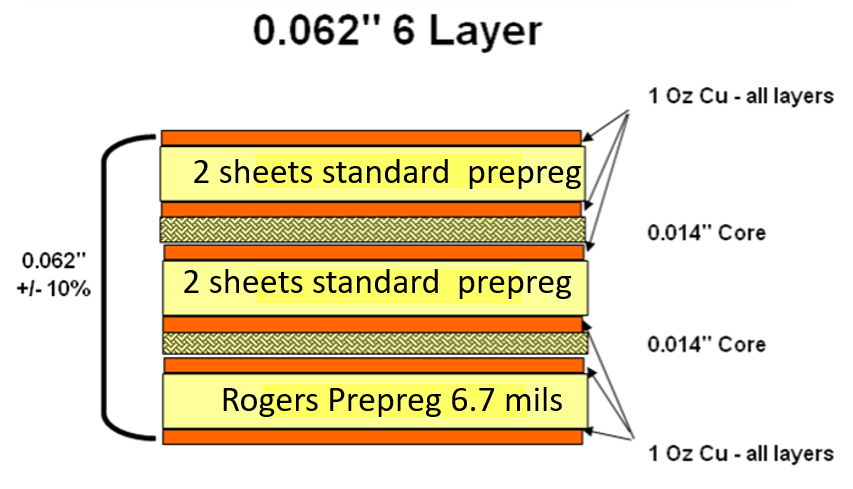
Characteristic impedance arises from the interplay of inductance and capacitance along a transmission line, governed by geometry and material properties. In microstrip configurations, the signal trace sits atop the dielectric with air above, resulting in an effective dielectric constant lower than the substrate's nominal value. Stripline places the trace between two ground planes, fully embedded in dielectric for higher shielding and predictable behavior. Both microstrip impedance and stripline impedance depend on trace width, thickness, substrate height, and dielectric constant. Engineers must differentiate between process dielectric constant, used in fabrication, and design dielectric constant for modeling accuracy. These principles form the foundation for controlled impedance PCB layouts.
Transmission line theory models these as distributed parameters, where impedance Z0 equals sqrt(L/C), with L as inductance per unit length and C as capacitance per unit length. Variations in copper roughness or dielectric anisotropy alter these values, particularly above gigahertz frequencies. Rogers substrates mitigate such issues through low-loss formulations and dimensional stability. Calculations incorporate corrections for conductor thickness and proximity effects in differential pairs. Adhering to IPC-2141 guidelines ensures designs account for manufacturing tolerances in trace etching and plating. This standard provides equations tailored for high-speed controlled impedance circuit boards.
Microstrip Impedance Fundamentals
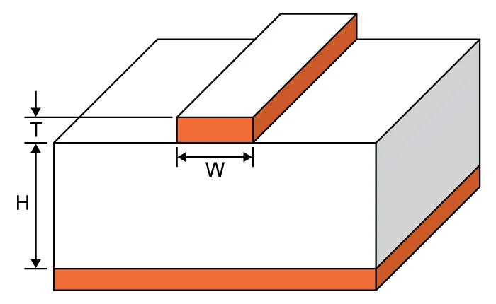
Microstrip lines suit surface routing where heat dissipation and probe access matter. The impedance formula integrates width-to-height ratio, adjusted for fringing fields at edges. Engineers input trace width W, substrate height H, copper thickness T, and dielectric constant Er into the Rogers PCB impedance calculator. Effective Er blends substrate and air contributions, typically 0.6 to 0.7 times nominal Er. Narrower traces yield higher impedance, while wider ones lower it for given heights. Manufacturing constraints limit minimum widths to avoid open circuits during etching.
Practical designs balance impedance with density, often targeting 50 ohms for RF signals. Changes in stack-up height directly impact capacitance, requiring iterative calculator runs. Surface roughness on Rogers copper foils minimally affects skin effect losses compared to electrolytic foils. Validation involves time-domain reflectometry post-fabrication to confirm targets. Consistent ground plane stitching prevents cavity resonances that skew microstrip impedance.
Stripline Impedance Characteristics
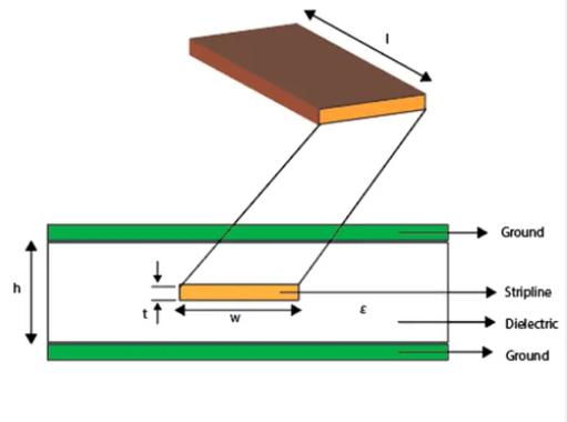
Stripline offers superior isolation, ideal for dense inner layers in controlled impedance PCBs. Symmetric placement between planes equalizes fields, simplifying impedance predictions. The calculator solves for width given total height between planes, split equally above and below the trace. Higher dielectric filling raises capacitance, lowering impedance for equivalent geometries versus microstrip. Engineers adjust for asymmetric stacks by weighting plane distances. This configuration shines in broadband applications with minimal radiation.
Fabrication demands uniform dielectric thickness to avoid impedance gradients along the line. Vias through stripline layers require stub management or back-drilling for continuity. IPC-2141 equations include factors for finite ground plane widths, enhancing accuracy. Rogers materials maintain low variation in Er across the board, supporting tight tolerances. Differential striplines double pair spacing for 100-ohm common-mode rejection.
Using a Rogers PCB Impedance Calculator: Step-by-Step
Start by defining target impedance, single-ended or differential, based on component specs. Gather material data: design Er from datasheets, typically stable for Rogers laminates. Specify stack-up: layer count, core/prepreg thicknesses, and plane assignments. Input trace parameters into the Rogers PCB impedance calculator: width guess, T=35um standard, frequency for loss models. Iterate width until Z0 matches within tolerance, noting effective Er output. Export results to layout tools for routing constraints.
Account for manufacturing: etching tolerance plus 10-20 percent width adjustment for pullback. Simulate bends and transitions using field solvers for validation. Differential pairs require edge-coupled calculations, emphasizing gap control. Document specs in fab drawings, specifying test coupons for TDR verification. This workflow ensures PCB impedance matching from design to assembly.
Best Practices for PCB Impedance Matching on Rogers Substrates
Prioritize stack-up optimization early, minimizing height variations across layers. Use continuous reference planes under high-speed traces, avoiding splits longer than wavelength fractions. Route pairs with constant width and spacing, minimizing vias. Length-match critical nets within eye diagram budgets. Select Rogers cores with matched CTE to copper for reliability under thermal cycling.
Tolerance budgeting combines material Er variation, usually under 2 percent for Rogers, with fab processes. Specify impedance test points on panels per IPC guidelines. Post-etch bake stabilizes dimensions before measurement. For mixed stacks, hybrid calculations blend FR-4 and Rogers properties accurately.
Troubleshooting Impedance Discrepancies
Measured impedances deviating from calculations often stem from inaccurate Er or height data. Verify fab drawings against as-built cross-sections via microsectioning. Excessive copper weight increases effective thickness, lowering Z0; compensate in models. Dielectric voids or delamination raise effective air content, spiking impedance. Recalibrate using fab-supplied test coupons before full-panel TDR.
Frequency-dependent losses manifest as rising Z0 at microwave bands; Rogers low-loss mitigates this. Differential imbalances from unequal gaps cause mode conversion. Iterative solver runs with measured Er refine future designs.
Conclusion
Mastering the Rogers PCB impedance calculator unlocks precise control over microstrip impedance, stripline impedance, and overall PCB impedance matching. Logical application of principles from IPC-2141 ensures controlled impedance PCB success in high-frequency realms. Engineers benefit from structured inputs, iterative refinement, and verification practices outlined here. Integrating these into workflows reduces signal integrity risks and accelerates time-to-market. For demanding RF and high-speed digital boards, this tool proves indispensable.
FAQs
Q1: What is a Rogers PCB impedance calculator used for?
A1: A Rogers PCB impedance calculator determines trace dimensions for target characteristic impedances in high-frequency designs using Rogers materials. Engineers input dielectric constant, heights, and widths to compute microstrip impedance or stripline impedance accurately. It accounts for effective Er blending, aiding controlled impedance PCB layouts. This prevents mismatches that cause reflections in RF signals. Typical outputs guide fab specs with 10 percent tolerances.
Q2: How does PCB impedance matching differ on Rogers substrates?
A2: PCB impedance matching on Rogers involves stable low-loss dielectrics for precise microstrip and stripline calculations. Unlike standard materials, Rogers maintains consistent Er over frequencies, simplifying Rogers PCB impedance calculator use. Focus on stack-up heights and plane integrity to hit 50 or 100 ohm targets. Manufacturing tolerances benefit from low CTE matching. Verification via TDR confirms integrity.
Q3: What factors affect controlled impedance PCB calculations?
A3: Key factors include trace width, substrate height, copper thickness, and design Er in controlled impedance PCB designs. Rogers PCB impedance calculator iterations adjust for these to achieve uniform Z0. Ground plane proximity and roughness influence results per IPC-2141. Frequency effects demand broadband models. Fab variations like etch control require tolerance margins.
Q4: Why choose stripline over microstrip for impedance control?
A4: Stripline provides better shielding and predictability for controlled impedance PCB inner layers compared to exposed microstrip. Fully dielectric-embedded traces minimize radiation and Er effective variations. Rogers PCB impedance calculator yields narrower widths for the same Z0 due to higher capacitance. Ideal for dense, high-speed routing. Drawbacks include via complexity.
References
IPC-2141 — Controlled Impedance Circuit Boards and High Speed Logic Design. IPC.
IPC-2221 — Generic Standard on Printed Board Design. IPC.
IPC-6012E — Qualification and Performance Specification for Rigid Printed Boards. IPC, 2017.


