Introduction
Designing and routing circuits on a 4-layer PCB offers electronic hobbyists a significant step up from simpler 2-layer boards. This approach provides more space for complex designs, better signal integrity, and improved power distribution. For those venturing into DIY electronics, mastering 4-layer PCB routing can transform a project from a basic prototype to a reliable, high-performance device. This guide aims to simplify the process with a practical focus on easy PCB layout techniques. Whether you are building a custom microcontroller board or experimenting with sensors, understanding the fundamentals of 4-layer PCB routing ensures your circuits function as intended. Let us explore the essential principles, best practices, and actionable tips to help hobbyists navigate this process with confidence while adhering to widely recognized industry standards for quality and performance.
What Is a 4-Layer PCB and Why It Matters
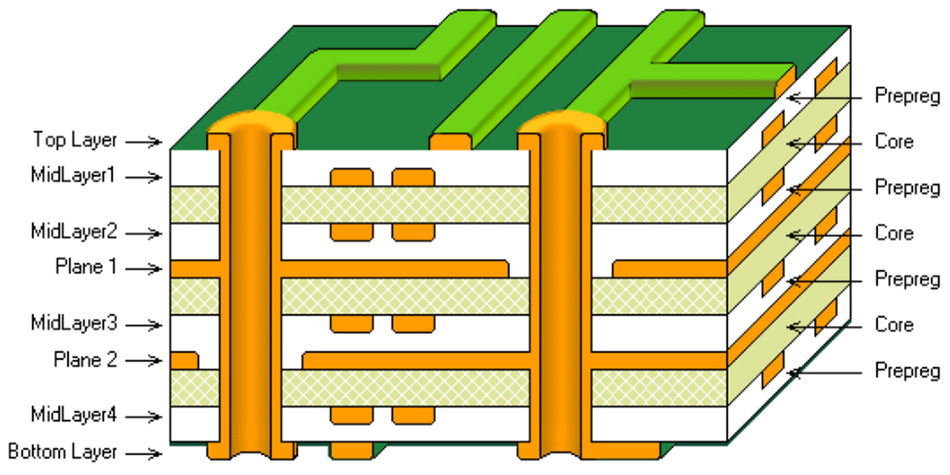
A 4-layer PCB consists of four conductive copper layers stacked with insulating material between them. Typically, the layers are arranged as top signal, ground plane, power plane, and bottom signal. This structure allows for more routing options compared to 2-layer boards, making it ideal for compact designs in DIY electronics. The additional layers help separate signals from power and ground, reducing interference and improving performance in circuits with moderate complexity.
For hobbyists, 4-layer PCB routing matters because it supports denser component placement and minimizes issues like crosstalk or electromagnetic interference. Projects involving microcontrollers, RF modules, or high-speed digital signals benefit greatly from this setup. Moreover, it provides a pathway to learn professional design techniques while keeping layouts manageable. Adopting this method prepares you for more advanced projects and ensures your creations meet functional and reliability expectations in real-world use.
Technical Principles of 4-Layer PCB Routing
Understanding the core principles behind 4-layer PCB routing is essential for creating effective layouts. The primary advantage of a 4-layer board lies in its stackup, which typically dedicates internal layers to ground and power planes. This configuration creates a shield against noise and provides a stable reference for signals on the outer layers.
Signal integrity is a key concern. High-speed signals, even in hobbyist projects, can suffer from reflections or delays if traces are too long or improperly routed. Keeping traces short and direct on the top and bottom layers helps maintain performance. The ground plane, often on layer 2, acts as a return path for signals, reducing loop areas that could pick up interference. Similarly, the power plane on layer 3 ensures consistent voltage delivery to components, avoiding drops or spikes.
Layer assignment also plays a critical role. Sensitive analog signals should avoid crossing digital traces to prevent noise coupling. Industry standards like IPC-2221B, which covers generic design principles for printed boards, emphasize maintaining separation between different signal types. Following such guidelines ensures that hobbyists achieve reliable operation without deep expertise in electromagnetic theory.
Best Practices for Easy PCB Layout on 4-Layer Boards
Routing a 4-layer PCB as a hobbyist requires a balance between simplicity and adherence to good design practices. Below are practical steps to achieve an effective and easy PCB layout while focusing on 4-layer PCB routing for DIY electronics.
Define Your Stackup Early
Start by confirming the layer arrangement. A common setup for hobbyists is signal on top, ground on layer 2, power on layer 3, and signal on the bottom. This structure simplifies routing and provides natural shielding. Ensure the ground plane is continuous under critical signal areas to minimize noise, as recommended by standards like IPC-2221B for optimal board performance.
Plan Component Placement First
Before routing, place components logically. Group related parts, such as decoupling capacitors near IC power pins, to shorten trace lengths. Position high-speed components to avoid long signal paths crossing over splits in ground planes. Thoughtful placement reduces routing complexity and enhances circuit stability, making the process more approachable for beginners in DIY electronics.
Route Power and Ground Connections
Focus on connecting power and ground first. Use the dedicated internal planes for these nets to ensure low impedance paths. Place vias strategically to connect components to these planes, avoiding unnecessary interruptions. A solid ground plane, as highlighted in industry practices, is crucial for reducing electromagnetic interference in a 4-layer PCB routing setup.
Keep Signal Traces Short and Direct
When routing signals on the top and bottom layers, aim for the shortest possible paths. Avoid sharp angles; use 45-degree turns instead of 90-degree corners to prevent signal reflections. If a trace must switch layers, place a via near the component pin to maintain a clean return path through the ground plane. This approach aligns with basic signal integrity principles.
Separate Analog and Digital Signals
If your project includes both analog and digital components, route them on different areas of the board. Keep analog traces away from noisy digital lines to prevent interference. Standards like IPC-2221B suggest maintaining physical separation or using ground plane barriers to isolate these signals, ensuring a reliable easy PCB layout.
Use Vias Wisely
Vias are essential in 4-layer PCB routing to connect traces between layers. However, excessive vias can disrupt ground planes and introduce noise. Limit their use and place them away from high-speed signal paths. When unavoidable, ensure nearby ground vias maintain a return path, preserving signal quality.
Common Challenges and Troubleshooting Tips
Even with careful planning, hobbyists may encounter issues during 4-layer PCB routing. One frequent problem is signal crosstalk, where adjacent traces interfere with each other. To mitigate this, increase spacing between critical traces and ensure a solid ground plane beneath them. Standards such as IPC-2221B provide guidance on minimum spacing to avoid such issues.
Another challenge is managing power distribution. Voltage drops can occur if power traces or planes are insufficient. Adding decoupling capacitors near power pins of ICs helps stabilize voltage levels. Inspecting the layout for thin or broken plane areas can prevent unexpected performance issues in DIY electronics projects.
Thermal management is also worth considering. Components generating heat, like voltage regulators, may require additional copper pours connected to the ground plane for dissipation. While hobbyist projects often operate at low power, ensuring proper heat distribution prevents long-term reliability concerns.
If a design fails to work as expected, check for routing errors. Verify that no critical traces cross plane splits, as this can disrupt return paths. Use continuity testing to confirm connections to ground and power planes. These steps often resolve basic issues without requiring advanced diagnostic tools.
Practical Example: Routing a Simple Microcontroller Circuit
Consider a basic project involving a microcontroller with a few sensors and LEDs. Start by placing the microcontroller centrally on the top layer for easy access to pins. Position sensors and LEDs around it, keeping related components close to minimize trace lengths. Connect power and ground pins to the internal planes using vias near the microcontroller.
Route digital signals, like SPI or I2C lines for sensors, on the top layer with short, direct traces. If space constraints force a layer change, add vias and ensure a nearby ground via for return current. LEDs and their resistors can be routed on the bottom layer to free up space, maintaining separation from sensitive sensor lines.
Finally, inspect the ground plane for interruptions caused by vias or cuts. Fill any gaps with additional vias to maintain continuity. This simple approach demonstrates how 4-layer PCB routing can be applied to everyday hobbyist projects, ensuring functionality and reliability.
Conclusion
Routing simple circuits on a 4-layer PCB offers electronic hobbyists a powerful way to enhance their DIY electronics projects. By leveraging the additional layers for ground and power planes, you can achieve better signal integrity and reduced interference compared to simpler boards. This guide has outlined the technical principles, best practices, and troubleshooting tips to make 4-layer PCB routing accessible. From defining a proper stackup to separating signal types, each step contributes to an easy PCB layout that performs reliably. Following industry standards like IPC-2221B ensures your designs meet accepted quality benchmarks. With practice, these techniques will become second nature, empowering you to tackle more complex designs with confidence and precision in your future endeavors.
FAQs
Q1: What are the main benefits of 4-layer PCB routing for hobbyists?
A1: For hobbyists, 4-layer PCB routing provides more space for complex circuits and improves signal quality. It reduces noise through dedicated ground and power planes, making projects like microcontroller boards more reliable. This setup also allows compact designs without sacrificing performance, ideal for DIY electronics enthusiasts looking to elevate their skills and build professional-grade prototypes.
Q2: How can I achieve an easy PCB layout on a 4-layer board?
A2: Achieving an easy PCB layout starts with a clear stackup, placing components logically, and routing power and ground first. Keep signal traces short, use vias sparingly, and separate analog and digital signals. Following basic guidelines from standards like IPC-2221B helps simplify the process, ensuring a manageable design for hobbyists working on DIY electronics.
Q3: What tools are best for a PCB routing tutorial on 4-layer designs?
A3: Many free and accessible design software options support 4-layer PCB routing tutorials for hobbyists. Look for tools with layer management features and design rule checks to guide your layout. Focus on learning core routing principles, such as signal separation and plane usage, to build skills applicable across different platforms in DIY electronics.
Q4: How do I avoid common mistakes in 4-layer PCB routing?
A4: Avoid common mistakes in 4-layer PCB routing by planning component placement carefully and maintaining solid ground planes. Do not cross sensitive traces over plane splits, and keep vias minimal to prevent noise. Regularly review your design against standards like IPC-2221B to catch errors early, ensuring a functional layout for your projects.
References
IPC-2221B — Generic Standard on Printed Board Design. IPC, 2012.


