Introduction
Signal integrity remains a critical concern in modern high-speed PCB designs, where data rates exceeding several gigabits per second amplify issues like reflections, crosstalk, and attenuation. Engineers designing for applications such as telecommunications, computing, and automotive systems must address these challenges to ensure reliable signal transmission. Leveraging 3 oz copper PCBs offers a strategic advantage by providing thicker copper layers that reduce resistive losses and support robust current handling without compromising performance. This thickness, equivalent to approximately 105 micrometers, contrasts with standard 1 oz copper at 35 micrometers, enabling better management of high-frequency signals. In high speed PCB design, 3 oz copper PCB signal integrity becomes particularly valuable as it minimizes PCB signal loss over long traces. By understanding how to integrate this material effectively, designers can achieve cleaner eye diagrams and lower bit error rates.
The shift toward denser interconnects and faster edge rates demands precise control over transmission line characteristics. Traditional thinner copper layers often lead to higher attenuation at frequencies above 1 GHz, degrading signal quality. 3 oz copper mitigates this by lowering the DC resistance of traces, which directly impacts conductor loss. Moreover, it facilitates PCB impedance matching through adjusted geometries, a key factor in preventing reflections. PCB trace routing strategies must evolve accordingly to leverage these benefits fully. This article explores the principles, best practices, and practical insights for optimizing signal integrity with 3 oz copper PCBs.
Understanding Signal Integrity and the Role of 3 oz Copper in High-Speed Designs
Signal integrity refers to the ability of electrical signals to propagate through a PCB without distortion from noise, reflections, or attenuation. In high-speed environments, rapid rise times and high frequencies make the PCB itself a primary source of degradation. Why does 3 oz copper matter? Its increased thickness reduces the series resistance per unit length, which is crucial for maintaining signal amplitude over distance. This directly enhances 3 oz copper PCB signal integrity by combating PCB signal loss mechanisms prevalent in high speed PCB design.
Engineers encounter challenges like insertion loss, which increases with frequency due to skin effect and surface roughness. Thinner copper exacerbates this, as the effective conducting area diminishes at high frequencies. 3 oz copper provides a larger cross-sectional area, lowering overall attenuation even as skin depth limits penetration. Industry relevance grows with standards like IPC-2221, which guide conductor sizing and spacing to support reliable high-speed performance. Without such optimizations, systems suffer from increased jitter and reduced margins.
The economic and performance drivers for adopting 3 oz copper include not only loss reduction but also improved thermal management during operation. High-speed signals generate heat through I2R losses, and thicker copper dissipates it more effectively. This stability preserves dielectric properties, further aiding signal fidelity. Procurement teams value this for long-term reliability in demanding applications.
Technical Principles of Signal Integrity in 3 oz Copper PCBs
Conductor loss dominates PCB signal loss in high-speed designs, modeled as α_c = (R_s / (2 Z_0 w)), where R_s is surface resistivity, Z_0 is characteristic impedance, and w is trace width. Skin effect confines current to the conductor surface, with depth δ ≈ 66 / sqrt(f) micrometers at frequency f in GHz. For signals up to 10 GHz, δ exceeds 20 micrometers, so 3 oz copper's 105 micrometer thickness utilizes more of the cross-section compared to 1 oz. This reduces effective R_s and thus PCB signal loss, preserving signal power.
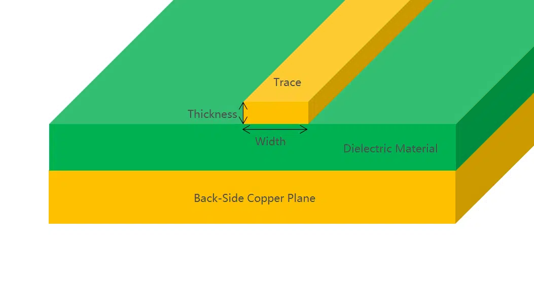
Dielectric loss, proportional to tan δ and sqrt(f), interacts with conductor effects, but thicker copper shifts the balance favorably. Impedance arises from distributed L and C per unit length; microstrip Z_0 ≈ (87 / sqrt(ε_r + 1.41)) * ln(5.98 h / (0.8 w + t)), where h is dielectric height, w trace width, t copper thickness. Increased t lowers Z_0 for fixed w and h, necessitating wider traces or thinner dielectrics for controlled 50-ohm or 100-ohm differential lines in PCB impedance matching.
Surface roughness adds to loss via increased effective path length, quantified by the roughness factor in models. Smoother plating on 3 oz copper minimizes this penalty. Electromagnetic coupling via crosstalk scales with trace proximity; thicker copper's rigidity aids consistent spacing. These principles underscore why 3 oz copper excels in high speed PCB design.
Achieving PCB Impedance Matching with 3 oz Copper
PCB impedance matching ensures maximum power transfer and minimal reflections, quantified by return loss RL = -20 log(|Γ|), where Γ = (Z_L - Z_0)/(Z_L + Z_0). Mismatches cause ringing and overshoot, degrading eye height. With 3 oz copper, the thicker t requires compensation: for microstrip, increase w proportionally or reduce h. Simulations confirm that a 20% t increase demands 10-15% wider traces for constant Z_0.
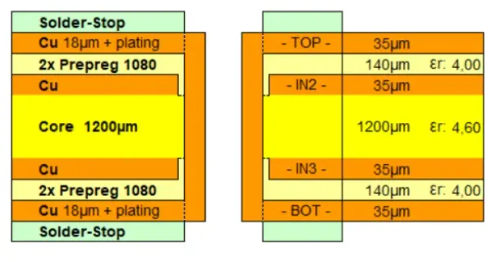
Stackup design plays a pivotal role, placing high-speed traces on outer layers with dedicated reference planes. Asymmetric buildup from thick copper demands symmetric cores to avoid skew. Tolerance control per IPC-6012 specifications ensures repeatability, as ±10% Z_0 variation doubles reflections. Differential pairs benefit from tight coupling, with intra-pair spacing s ≈ 2w for 100 ohms.
Via transitions disrupt matching; stub effects add inductance. Back-drilling or blind vias mitigate this in 3 oz designs. Fabricators specify etch factors, as thicker copper yields trapezoidal profiles affecting Z_0 by 5-10%.
Best Practices for PCB Trace Routing in High-Speed 3 oz Copper Designs
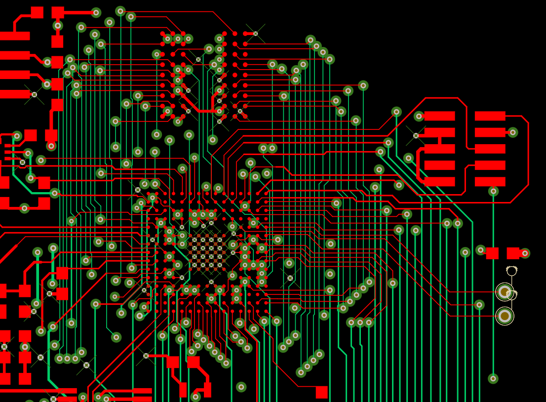
PCB trace routing demands length matching within 1/20th rise time to avoid skew. For 100 ps rise time, limit less than 5 mm mismatch. Route differential pairs broadside or edge-coupled with constant spacing, avoiding bends greater than 45 degrees to minimize mode conversion. In 3 oz copper, minimum widths exceed 10 mils due to etch limits, increasing crosstalk risk; space traces greater than 3h apart.
Use ground planes beneath signals for return path integrity, minimizing loop inductance. Avoid splitting planes under traces to prevent impedance discontinuities. Vias introduce 1-2 nH each; minimize count and stagger them. Serpentine routing equalizes lengths without sharp turns.
Power integrity couples with signal; wide 3 oz planes reduce droop. Per IPC-2221, annular rings greater than 2x drill size prevent breakout. Test coupons verify Z_0 post-fabrication.
Mitigating PCB Signal Loss in Practice
Total loss IL = α_c + α_d, with α_c scaling as sqrt(f)/w and α_d as f tan δ. 3 oz copper halves α_c versus 1 oz for same w, extending reach by 50% at 5 GHz. Optimize via low-loss dielectrics (Dk less than 3.5, tan δ less than 0.005).
Routing minimizes vias and bends, which add 0.5-1 dB loss each. Pre-emphasis at drivers compensates known loss profiles. Thermal rise warps traces, altering Z_0; 3 oz rigidity resists this.
Troubleshooting Common Issues in 3 oz Copper High-Speed Designs
Excessive jitter often traces to ground bounce; solidify stitching vias around perimeters. Crosstalk spikes indicate inadequate spacing; measure near/far-end with TDR. Insertion loss exceeding 1 dB/inch flags roughness; specify RTF plating. Warpage from CTE mismatch stresses traces; balance Cu distribution.
Iterate stackups in field solvers, correlating with VNA measurements. IPC-6012 performance specs guide acceptance.
Conclusion
Leveraging 3 oz copper PCBs elevates signal integrity in high-speed designs by slashing conductor losses and enabling precise impedance control. Key strategies include optimized trace geometries, meticulous routing, and adherence to standards like IPC-2221. PCB impedance matching and PCB trace routing practices ensure reflections stay below -20 dB, while reduced PCB signal loss supports longer channels. Designers achieve robust high speed PCB design outcomes through these methods. Future trends toward 50+ Gbps will amplify the value of thick copper solutions.
FAQs
Q1: What role does 3 oz copper play in PCB signal integrity for high-speed applications?
A1: 3 oz copper reduces resistive losses due to its 105 micrometer thickness, lowering attenuation from skin effect and DC resistance. This preserves signal amplitude in high speed PCB design, improving eye opening. Routing must account for wider minimum features to maintain PCB impedance matching. Overall, it extends reliable transmission distances compared to thinner foils.
Q2: How does PCB impedance matching impact high speed PCB design with 3 oz copper?
A2: Thicker copper lowers characteristic impedance for given geometry, requiring wider traces or adjusted stackups to hit 50 or 100 ohms. Mismatches amplify reflections, causing jitter. Control tolerances to ±10% via precise etch control. This ensures clean signal propagation in demanding environments.
Q3: What are best practices for PCB trace routing in 3 oz copper for signal integrity?
A3: Maintain length matching, use 45-degree bends, and space traces greater than 3 times dielectric height. Minimize vias with back-drilling. Pair routing preserves differential balance. These steps, aligned with IPC-2221, curb crosstalk and discontinuities.
Q4: How can engineers minimize PCB signal loss in 3 oz copper designs?
A4: Select low tan δ dielectrics, smooth copper surfaces, and shorten paths. Thicker copper inherently cuts conductor loss. Verify with coupons and simulations. Balanced power planes aid return currents.
References
IPC-2221 — Generic Standard on Printed Board Design. IPC
IPC-6012 — Qualification and Performance Specification for Rigid Printed Boards. IPC
IPC-A-600 — Acceptability of Printed Boards. IPC


