Introduction
For electronic hobbyists venturing into PCB prototyping, signal integrity stands as a critical factor that can make or break a design. Whether you are working on a simple breadboard PCB design or a complex multilayer project, maintaining signal quality during prototyping is essential for ensuring functionality. Different stackup options in PCB design play a significant role in managing signal integrity, especially when dealing with high-speed signals or noise-sensitive circuits. This article explores practical tips for achieving optimal signal quality prototyping by understanding and selecting appropriate stackup configurations. From basic two-layer boards to more advanced multilayer setups, hobbyists can apply these insights to enhance their DIY electronics prototyping projects. Let’s dive into the fundamentals and actionable strategies for maintaining signal integrity.
What Is Signal Integrity and Why It Matters in PCB Prototyping
Signal integrity refers to the ability of an electrical signal to maintain its quality as it travels through a circuit, without distortion or interference. In the context of rapid PCB prototyping signal integrity, this means ensuring that signals remain clear and reliable from one component to another. Poor signal integrity can lead to issues like crosstalk, electromagnetic interference, or data loss, which are particularly problematic in high-speed or sensitive designs.
For electronic hobbyists, signal integrity matters because it directly impacts the performance of a prototype. A distorted signal in a DIY electronics prototyping project could result in malfunctioning circuits or inaccurate sensor readings. Understanding how to manage signal quality during prototyping helps hobbyists validate their designs before moving to full production. It also builds a foundation for learning advanced concepts, such as impedance matching and noise reduction, which are crucial for complex projects.
Technical Principles of Signal Integrity in PCB Design
Signal integrity in PCB prototyping is influenced by several technical factors. These include trace routing, layer arrangement, and the materials used in the board. Let’s break down the key principles that hobbyists should understand.
First, signal paths must be as short and direct as possible to minimize delay and loss. Longer traces can introduce parasitic inductance and capacitance, degrading signal quality. Second, crosstalk occurs when signals on adjacent traces interfere with each other, often due to poor spacing or lack of shielding. Third, impedance mismatches can cause signal reflections, especially in high-speed designs, leading to errors in data transmission.
Stackup options prototyping plays a pivotal role in addressing these issues. A stackup refers to the arrangement of conductive and insulating layers in a PCB. For instance, a two-layer board typically has signals on both layers, while a four-layer board might dedicate inner layers to ground and power planes. These planes help reduce noise by providing a stable reference for signals and shielding against interference. According to industry standards like IPC-2221B, proper stackup design is essential for controlling impedance and minimizing electromagnetic interference in multilayer boards.
Suggested Reading: Enhancing USB Performance: A Guide to Optimal PCB Layout and Signal Integrity
Impact of Stackup Options on Signal Quality Prototyping
Different stackup configurations directly affect signal quality prototyping. Hobbyists often start with breadboard PCB design or simple two-layer boards due to cost and simplicity. However, these setups can struggle with signal integrity in high-speed or noise-sensitive applications. Let’s explore common stackup options and their impact.
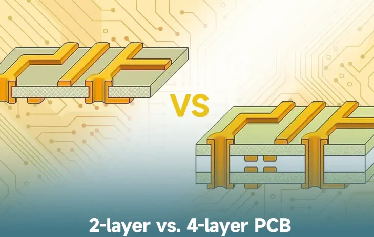
Two-Layer Stackup
A two-layer stackup is the most basic and affordable option for hobbyists. Signals are routed on both the top and bottom layers, often with no dedicated ground or power planes. While suitable for low-speed circuits, this configuration is prone to noise and crosstalk because there is no shielding between traces. To mitigate issues, hobbyists should maximize trace spacing and avoid running high-speed signals parallel to each other for long distances.
Four-Layer Stackup
A four-layer stackup offers better signal integrity by incorporating dedicated ground and power planes in the inner layers. This setup reduces electromagnetic interference and provides a stable reference for signals on the outer layers. For DIY electronics prototyping involving microcontrollers or moderate-speed signals, a four-layer board can significantly improve performance. The ground plane also helps with heat dissipation, which is an added benefit.
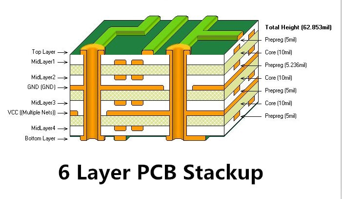
Six-Layer and Beyond
For advanced projects, a six-layer stackup or higher might be necessary. These configurations allow for multiple signal layers separated by ground and power planes, offering excellent noise isolation. Such stackups are ideal for high-speed digital circuits or mixed-signal designs where analog and digital signals must coexist without interference. While more expensive, they are worth considering for complex prototypes.
Practical Solutions for Maintaining Signal Integrity in Prototyping
Achieving good PCB prototyping signal integrity requires practical strategies tailored to the stackup being used. Below are actionable tips for hobbyists working on breadboard PCB design or custom prototypes.
Optimize Trace Routing
Keep traces as short and direct as possible to reduce signal delay and loss. Avoid sharp corners in routing, as they can cause signal reflections. Instead, use 45-degree angles or smooth curves. For two-layer boards, try to route critical signals on one layer and use the other for ground connections to mimic a pseudo-ground plane.
Use Ground Planes Effectively
Whenever possible, incorporate a ground plane in your stackup. A continuous ground plane beneath signal traces provides a low-impedance return path, reducing noise. In a two-layer design, dedicate as much area as possible to ground pours on both layers. For multilayer boards, follow guidelines from IPC-2221B to ensure proper placement of ground and power planes.
Control Impedance for High-Speed Signals
Impedance matching is crucial for high-speed signals to prevent reflections. Calculate the required trace width and spacing based on the dielectric constant of your board material and the target impedance. Many free online tools can assist with these calculations for hobbyists. In multilayer stackups, ensure that signal layers are adjacent to a reference plane to maintain consistent impedance.
Minimize Crosstalk
Crosstalk can be reduced by increasing the spacing between parallel traces. A general rule is to keep spacing at least three times the trace width. In multilayer stackups, route high-speed signals on different layers separated by a ground plane to further isolate them. This approach is particularly effective in four-layer or higher configurations.
Select Appropriate Materials
The choice of substrate material impacts signal integrity. Standard FR-4 material is sufficient for most hobbyist projects, but for high-frequency designs, consider materials with lower dielectric loss. Ensure that the material properties align with the stackup design to avoid impedance variations.
Troubleshooting Common Signal Integrity Issues
Even with careful planning, signal integrity issues can arise during PCB prototyping. Hobbyists should be prepared to identify and resolve common problems. If signals appear noisy or distorted, check for long parallel traces that might cause crosstalk. Use an oscilloscope, if available, to observe signal waveforms and pinpoint interference sources.
Another frequent issue is signal reflection due to impedance mismatch. Verify that trace widths and layer spacing conform to the calculated values for your design. If using a two-layer board, consider upgrading to a four-layer stackup for better control over impedance and noise. Ground loops are also a concern, especially in breadboard PCB design. Ensure that ground connections form a single, continuous path without loops that can act as antennas for noise.
Conclusion
Maintaining signal integrity during PCB prototyping is a fundamental skill for electronic hobbyists. By understanding the principles of signal quality prototyping and exploring different stackup options prototyping, you can significantly improve the performance of your designs. Whether working with a simple two-layer breadboard PCB design or a complex multilayer setup, practical strategies like optimizing trace routing, using ground planes, and controlling impedance are within reach. These tips, grounded in industry standards such as IPC-2221B, empower hobbyists to tackle signal integrity challenges in DIY electronics prototyping. With careful planning and troubleshooting, your prototypes can achieve reliable and accurate results, paving the way for successful projects.
FAQs
Q1: How can I improve PCB prototyping signal integrity on a two-layer board?
A1: For a two-layer board, focus on keeping signal traces short and spaced apart to reduce crosstalk. Use ground pours on both layers to create a pseudo-ground plane. Avoid routing high-speed signals parallel for long distances. Following basic layout guidelines from standards like IPC-2221B can help hobbyists achieve better signal quality in simple designs.
Q2: What stackup options in prototyping are best for high-speed signals?
A2: For high-speed signals, a four-layer or six-layer stackup is ideal. These configurations allow dedicated ground and power planes, which shield signals and maintain impedance. Inner planes reduce noise and interference, making them suitable for complex DIY electronics prototyping projects where signal integrity is critical.
Q3: How does breadboard PCB design affect signal quality during prototyping?
A3: Breadboard PCB design often lacks proper grounding and shielding, leading to noise and crosstalk. Signals can degrade due to long, unoptimized paths. Hobbyists should minimize trace lengths and consider moving to a custom PCB with a defined stackup for better signal quality prototyping in critical applications.
Q4: Why is a ground plane important for signal integrity in PCB prototyping?
A4: A ground plane provides a low-impedance return path for signals, reducing noise and interference. It acts as a shield against electromagnetic interference, crucial for maintaining signal integrity. In multilayer stackups, ground planes enhance stability, making them essential for reliable PCB prototyping signal integrity.
References
IPC-2221B — Generic Standard on Printed Board Design. IPC, 2012.
IPC-6012E — Qualification and Performance Specification for Rigid Printed Boards. IPC, 2020.


