Introduction
In the fast-paced world of electronics, printed circuit boards (PCBs) must meet stringent performance requirements, especially for high-speed applications. Backdrilling, a critical technique in PCB fabrication, addresses signal integrity challenges by removing unused via stubs that can cause signal distortion. Simulating backdrilling before manufacturing ensures optimal design and prevents costly rework. This article explores the role of backdrilling simulation software, signal integrity simulation, and PCB simulation tools in achieving performance optimization. Aimed at electrical engineers, the content provides technical insights into simulation accuracy and practical steps to enhance PCB designs for high-speed systems.
What Is Backdrilling and Why It Matters
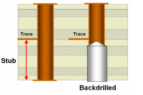
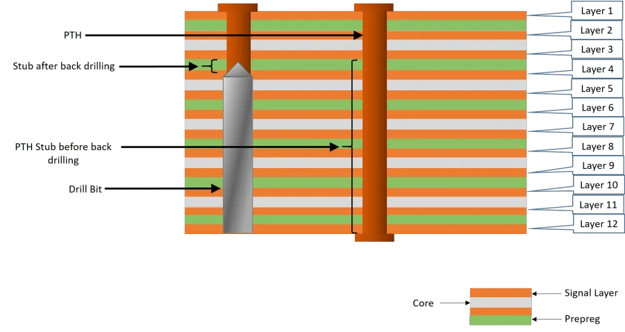
Backdrilling is a manufacturing process used to eliminate via stubs in multilayer PCBs. Via stubs are the unused portions of plated through holes that extend beyond the signal layer connection. These stubs can act as resonant structures, leading to signal reflections and degradation, particularly in high-speed designs operating at gigahertz frequencies. By drilling out these stubs, backdrilling minimizes impedance discontinuities and enhances signal integrity.
The importance of backdrilling grows as data rates increase in applications like telecommunications, data centers, and advanced computing. Without addressing via stubs, signal loss and crosstalk can compromise system reliability. Simulation of backdrilling allows engineers to predict and mitigate these issues during the design phase, reducing the risk of failures in the final product. Using PCB simulation tools to model backdrilling effects ensures that designs meet performance specifications before fabrication begins.
Technical Principles of Backdrilling and Signal Integrity
Backdrilling involves mechanically drilling out the excess via barrel after the initial plating process. This technique targets vias in multilayer boards where signals transition between layers, leaving only the necessary conductive path. The primary goal is to reduce the stub length, which directly impacts signal integrity by minimizing reflections and maintaining impedance control.
Signal integrity refers to the quality of an electrical signal as it travels through a PCB. Factors like impedance mismatch, crosstalk, and signal loss can degrade integrity, especially at high frequencies. Via stubs exacerbate these issues by acting as unintended antennas, causing resonance and distorting waveforms. Backdrilling addresses this by shortening the stub, aligning the via’s electrical length with the design requirements.
Simulation plays a pivotal role in understanding these interactions. Signal integrity simulation models the electrical behavior of vias, traces, and interconnects under various conditions. It helps engineers visualize how stub length affects signal propagation and identify optimal backdrilling depths. Accurate simulation requires precise input data, such as dielectric properties and layer stackup details, to reflect real-world performance. Standards like IPC-6012E provide guidelines for via fabrication and performance, ensuring that simulation parameters align with industry norms.
Role of Backdrilling Simulation Software in Design Optimization
Backdrilling simulation software enables engineers to model the effects of via stub removal on signal performance without physical prototypes. These tools integrate with broader PCB simulation platforms to analyze impedance, signal delay, and crosstalk in a virtual environment. By simulating backdrilling, designers can determine the precise depth and placement of drilled vias to achieve optimal results.
One key advantage of simulation is the ability to test multiple scenarios. Engineers can adjust stub lengths, via diameters, and layer transitions to observe their impact on signal integrity. This iterative process identifies potential issues, such as overdrilling or insufficient stub removal, before manufacturing begins. Simulation accuracy depends on the quality of the models and the software’s ability to replicate physical conditions, including material properties and manufacturing tolerances.
Beyond signal integrity, backdrilling simulation helps optimize manufacturing processes. It ensures that drilling parameters comply with design rules and minimizes the risk of damaging adjacent layers. Adhering to standards like IPC-A-600K for acceptability criteria ensures that simulated outcomes translate to reliable fabricated boards.

Practical Solutions for Backdrilling Performance Optimization
Achieving effective backdrilling performance optimization requires a systematic approach during the design and simulation phases. Below are actionable steps to integrate simulation into the PCB development workflow.
- Define Design Parameters: Start by specifying the layer stackup, via sizes, and signal requirements. Accurate stackup data ensures that simulations reflect the intended board configuration.
- Select Appropriate Tools: Use PCB simulation tools capable of modeling high-frequency effects and via structures. Ensure the software supports detailed analysis of impedance and signal propagation.
- Model Via Stubs: Input precise via dimensions and stub lengths into the simulation environment. Test various backdrilling depths to identify the configuration with minimal signal distortion.
- Validate Signal Integrity: Run signal integrity simulations to assess reflection, crosstalk, and loss. Compare results against performance targets to confirm design viability.
- Iterate and Refine: Adjust design parameters based on simulation outcomes. Repeat the process until optimal performance is achieved, balancing signal quality with manufacturing constraints.
Incorporating these steps reduces design iterations and enhances reliability. Simulation also aids in documenting compliance with standards like IPC-6012E, which specifies performance requirements for rigid boards.
Best Practices for Enhancing Simulation Accuracy
Simulation accuracy is critical to reliable backdrilling performance optimization. Inaccurate models can lead to incorrect predictions, resulting in design flaws or manufacturing defects. Follow these best practices to ensure precise results.
- Use Accurate Material Data: Input correct dielectric constants and loss tangents for PCB materials. These properties influence signal behavior at high frequencies.
- Account for Manufacturing Tolerances: Include variations in drilling depth and via plating thickness in simulations. This reflects real-world fabrication limits.
- Validate with Standards: Align simulation setups with industry guidelines, such as those in IPC-A-600K, to ensure acceptability of modeled structures.
- Cross-Verify Results: Compare simulation outputs with theoretical calculations or known benchmarks. Discrepancies may indicate modeling errors requiring correction.
Accurate simulations provide confidence in design decisions, minimizing the need for costly physical prototypes. They also enable engineers to address potential signal integrity issues proactively, ensuring robust PCB performance.
Challenges in Backdrilling Simulation and Mitigation Strategies
Despite its benefits, backdrilling simulation presents challenges that can affect outcomes. One common issue is the complexity of modeling multilayer structures with varying dielectric properties. Inaccurate assumptions about material behavior can skew results, leading to suboptimal designs.
Another challenge is balancing simulation detail with computational resources. High-fidelity models require significant processing power, potentially delaying design timelines. Simplifying models without sacrificing accuracy is essential for practical implementation.
To mitigate these issues, engineers should prioritize critical design areas for detailed simulation while using simplified models for less critical sections. Regular updates to material libraries and simulation algorithms also improve accuracy. Adhering to standardized testing methods, as outlined in IPC-6012E, ensures consistency between simulated and manufactured boards.
Conclusion
Simulating backdrilling is a powerful strategy for optimizing PCB performance before manufacturing. By leveraging backdrilling simulation software and signal integrity simulation, engineers can address via stub issues, enhance signal quality, and ensure design reliability. PCB simulation tools enable detailed analysis of high-speed designs, reducing the risk of failures and minimizing production costs. Following best practices for simulation accuracy and aligning with industry standards guarantees that virtual models translate to successful physical boards. For electrical engineers, integrating these techniques into the design workflow is essential for meeting the demands of modern electronics.
FAQs
Q1: How does backdrilling simulation software improve PCB design?
A1: Backdrilling simulation software models the removal of via stubs to predict their impact on signal integrity. It allows engineers to test various drilling depths and via configurations virtually, identifying optimal settings before manufacturing. This reduces design errors, enhances performance in high-speed applications, and saves time and cost by minimizing physical prototypes.
Q2: What factors affect simulation accuracy in PCB signal integrity analysis?
A2: Simulation accuracy depends on precise input data, including material properties, via dimensions, and layer stackup details. Manufacturing tolerances and environmental conditions also play a role. Using updated models and adhering to industry standards ensures reliable results, helping engineers trust the simulation for critical design decisions.
Q3: Why is signal integrity simulation critical for high-speed PCBs?
A3: Signal integrity simulation identifies issues like reflections and crosstalk caused by via stubs in high-speed PCBs. It ensures signals transmit without distortion, maintaining system reliability. By simulating these effects early, engineers can optimize designs, prevent failures, and meet performance requirements in demanding applications.
Q4: How can backdrilling performance optimization reduce manufacturing risks?
A4: Backdrilling performance optimization through simulation helps define precise drilling parameters, reducing the risk of overdrilling or damaging layers. It ensures vias meet signal integrity needs without compromising board structure. This proactive approach minimizes rework, lowers production costs, and improves overall manufacturing success rates.
References
IPC-6012E — Qualification and Performance Specification for Rigid Printed Boards. IPC, 2020.
IPC-A-600K — Acceptability of Printed Boards. IPC, 2020.


