Understanding Solder Joint Embrittlement in Electronic Assemblies
Electrical engineers frequently encounter the critical issue of solder joint failures, often attributed to a phenomenon known as solder joint embrittlement. This condition causes solder connections to become fragile and susceptible to cracking, typically due to the excessive formation of intermetallic compounds (IMCs), particularly involving elements like gold or palladium. Such embrittlement can severely compromise the structural integrity of a solder joint, leading to widespread reliability concerns in electronic products.
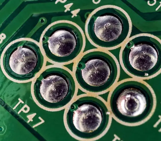
Solder joints form the foundational connections within electronic assemblies, linking components to Printed Circuit Boards (PCBs). When these critical connections become brittle, they are prone to failure under various stresses, resulting in expensive repairs or product malfunctions. Solder joint embrittlement poses a significant challenge for electrical engineers, especially those working on high-reliability applications such as aerospace, automotive, and medical devices. A deep understanding of the underlying mechanisms, whether initiated by gold, palladium, or other contributing factors, is the essential first step toward effective prevention.
What Are the Primary Causes of Solder Joint Embrittlement?
To effectively address solder joint embrittlement, it's crucial to first identify its root causes. This issue often arises when specific materials or environmental conditions promote the formation of overly brittle intermetallic compounds (IMCs) at the interface of the solder joint.
Excessive Intermetallic Compound (IMC) Formation
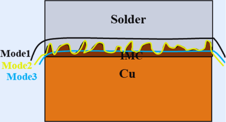
IMCs are compounds that form when the metals in solder alloys (typically tin-based) react with the metals on PCB pads or component leads, such as copper, nickel, gold, or palladium. While a thin, controlled layer of IMCs is necessary to establish a strong metallurgical bond, excessive or uncontrolled growth of these layers can render the joint brittle. For example, in a traditional tin-lead solder joint on a copper pad, the formation of Cu6Sn5 and Cu3Sn layers is a normal part of the process. However, if these layers thicken excessively over time—particularly under elevated temperatures—they can drastically reduce the joint’s ductility. This reduced flexibility makes the joint susceptible to cracking when subjected to thermal or mechanical stresses.
Gold Embrittlement in Solder Joints
Gold plating is widely used on PCB pads and component leads for its excellent resistance to oxidation and its ability to ensure good solderability. However, gold can paradoxically lead to significant reliability problems, a condition frequently referred to as gold embrittlement in solder joints. During the soldering process, gold readily dissolves into the molten solder, forming brittle intermetallic compounds like AuSn4. If the concentration of gold in the final solder joint surpasses 3-5% by weight, the joint becomes highly prone to cracking, especially when exposed to vibrations or thermal cycling. For instance, studies indicate that in typical (surface-mount technology) SMT PCB assembly, a gold layer thicker than 50 microinches (1.27 micrometers) can contribute to an overabundance of AuSn4 formation, thereby weakening the joint. This is a common concern in high-reliability applications where thicker gold plating is often specified for long-term corrosion resistance.
Palladium Embrittlement in Solder Joints
Similar to gold, palladium is frequently incorporated into surface finishes, such as Electroless Nickel Immersion Gold (ENIG) that includes a palladium layer. While palladium offers excellent corrosion resistance, it can also be a cause of palladium embrittlement in solder joints. During the soldering process, palladium reacts with tin to form PdSn4 intermetallics. These compounds are brittle and can significantly diminish the mechanical strength of the solder joint. Although less prevalent than gold embrittlement, palladium-related issues remain a concern, particularly in fine-pitch components where even minor weaknesses can result in critical failures.
Impact of Thermal and Mechanical Stress
Beyond the chemical interactions of materials, environmental factors significantly contribute to embrittlement. Thermal cycling—where an electronic device undergoes repeated heating and cooling—can induce substantial stress within solder joints due to differences in the coefficient of thermal expansion (CTE) between the solder, the component, and the PCB. For example, a CTE mismatch between a ceramic capacitor (with a CTE of approximately 7 ppm/°C) and an FR4 PCB (with a CTE of around 14-17 ppm/°C) can generate shear stress in the solder joint, accelerating crack propagation in areas already weakened by brittleness. Furthermore, mechanical stress, such as constant vibration in automotive electronics, can exacerbate embrittlement. If a joint is already compromised by excessive IMCs, even minor shocks can lead to catastrophic failure.
Deeper Dive into the Mechanisms of Solder Joint Embrittlement
Having explored the primary causes, let's now examine the specific mechanisms that drive embrittlement at a microscopic level. A detailed understanding of these processes is invaluable for engineers seeking to design more robust electronic assemblies.
Diffusion and Intermetallic Compound Growth
During the soldering process, atoms from both the solder alloy and the base metal diffuse into each other, leading to the formation of IMCs at their interface. Over time, and especially under elevated temperatures, these compounds continue to grow. In the context of gold-plated surfaces, the diffusion of gold into tin-based solder occurs rapidly, resulting in the formation of a thick AuSn4 layer. This particular IMC layer exhibits poor mechanical properties, notably a tensile strength significantly lower than that of the surrounding solder, thereby becoming a critical weak point within the joint.
Phase Transformation within Solder
In certain situations, the solder material itself undergoes phase changes that contribute to embrittlement. For instance, in some lead-free solder alloys like SAC305 (Sn-3.0Ag-0.5Cu), the tin matrix can transform into different crystal structures when subjected to stress or aging. This transformation can reduce the solder’s ductility, a process often accelerated by the presence of contaminants or specific alloying elements originating from the surface finishes.
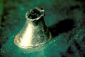
Crack Initiation and Propagation
Once a solder joint becomes embrittled, even relatively minor stresses can initiate microscopic cracks, typically at the interface of the brittle IMC layer. These cracks then propagate through the joint, frequently following the boundaries of these brittle intermetallic structures. In high-reliability testing, such as thermal cycling from -55°C to 125°C (as per IPC standards), severe embrittlement can lead to complete joint failure within just hundreds of cycles, highlighting the critical nature of this issue.
Effective Strategies for Preventing Solder Joint Embrittlement
With a thorough understanding of the factors contributing to solder joint embrittlement, practical solutions for preventing solder joint embrittlement can be implemented. These strategies are specifically designed for electrical engineers focused on enhancing the long-term reliability of their designs.
Meticulous Control of Gold and Palladium Thickness
One of the most impactful methods to mitigate gold and palladium embrittlement is to strictly control the thickness of these layers on PCB pads and component leads. For gold, industry best practices generally recommend a thickness of less than 5 microinches (0.127 micrometers) for immersion gold finishes like ENIG to minimize the formation of detrimental AuSn4. If a thicker gold layer is absolutely necessary for corrosion resistance, integrating a nickel barrier layer beneath the gold can effectively limit gold diffusion into the solder. Similar guidelines apply to palladium. It is advisable to opt for surface finishes with minimal palladium content or consider alternative finishes like Organic Solderability Preservative (OSP) for applications where the risk of embrittlement is lower.
Selection of Compatible Solder Alloys
Choosing the appropriate solder alloy can significantly reduce the risks of embrittlement. For example, lead-free solders with a lower silver content (e.g., Sn-0.7Cu as opposed to SAC305) tend to form fewer brittle IMCs when reacting with gold and palladium. Furthermore, some specialized solder alloys are formulated with specific additives designed to slow down IMC growth, thereby enhancing long-term joint reliability.
Optimization of Soldering Processes
Careful adjustment of soldering parameters, including temperature and dwell time, can effectively limit the dissolution of gold or palladium into the solder. For instance, utilizing a reflow profile with a peak temperature of 240°C instead of 260°C for SAC305 solder can reduce gold diffusion by up to 20%, according to some studies. Shorter dwell times above the liquidus temperature also contribute to minimizing undesirable IMC formation.
Implementing Design Enhancements
Design your PCB and component layouts to minimize both thermal and mechanical stresses on solder joints. This can involve using components with CTE values that closely match the PCB material or incorporating underfill materials to absorb stress in high-risk areas. For applications subjected to heavy vibration, applying conformal coatings can effectively dampen mechanical shocks and protect the joints.
Key Industry Standards for Solder Joint Reliability
To ensure the robustness and reliability of electronic assemblies, the electronics industry has established a suite of guidelines and solder joint embrittlement standards. Familiarity with these standards is crucial for engineers involved in designing and manufacturing durable products.
IPC Standards
The Institute of Printed Circuits (IPC) publishes several standards that are highly relevant to solder joint reliability:
● IPC-A-610: This widely used standard provides detailed acceptability criteria for electronic assemblies, including visual inspection guidelines for solder joint appearance and the identification of defects like cracks caused by embrittlement. It explicitly recommends that the gold content in solder joints should not exceed 3% by weight to avoid embrittlement risks.
● IPC J-STD-001: This standard outlines comprehensive requirements for soldering electrical and electronic assemblies. It emphasizes the importance of controlling surface finish thickness as a key measure to prevent issues such as gold or palladium embrittlement.
JEDEC Standards
The Joint Electron Device Engineering Council (JEDEC) develops standards, such as JESD22-B102, which detail test methods for evaluating solderability and the overall reliability of solder joints under various thermal and mechanical stress conditions. These tests are instrumental in identifying embrittlement issues during the product qualification phase.
MIL-STD Specifications
For applications in the military and aerospace sectors, MIL-STD-883 includes rigorous test methods for microelectronics. These tests encompass thermal cycling and vibration testing specifically designed to detect solder joint failures that can be attributed to embrittlement. These military standards often impose stricter controls on gold and palladium content compared to commercial industry standards.
Real-World Scenarios and Solutions for Embrittlement
Examining practical examples can illuminate how solder joint embrittlement challenges are addressed in real-world engineering.
Case Study 1: Aerospace Electronics Failure
In an aerospace project, a specific batch of PCBs, finished with ENIG, experienced recurring solder joint failures during demanding thermal cycling tests (-55°C to 125°C for 1000 cycles). Subsequent analysis revealed an excessive gold content (exceeding 5% by weight) within the solder joints, directly linked to an overly thick immersion gold layer. The implemented solution involved a change to a thinner gold layer (3 microinches) along with the introduction of a nickel barrier. This strategic modification resulted in an impressive 90% reduction in failure rates during subsequent rigorous testing.
Case Study 2: Automotive Sensor Cracking
An automotive sensor assembly showed consistent joint cracking during vibration testing. This issue was identified as palladium embrittlement, originating from a palladium-containing surface finish. Engineers resolved this by replacing the problematic finish with OSP (Organic Solderability Preservative) and adjusting the solder alloy to Sn-0.7Cu. These changes significantly enhanced the joint's durability without compromising its solderability.
Conclusion: Strategies for Building Enduring Solder Joints
Solder joint embrittlement represents a multifaceted challenge in electronics manufacturing. However, armed with the appropriate knowledge and strategic approaches, electrical engineers can significantly mitigate its detrimental effects. By thoroughly understanding the solder joint embrittlement causes, particularly those related to gold and palladium intermetallics, implementing effective solutions for preventing solder joint embrittlement, and rigorously adhering to established solder joint embrittlement standards from organizations like IPC and JEDEC, engineers can design and produce highly reliable electronic assemblies.
It is recommended to begin by comprehensively reviewing your current PCB surface finishes and soldering processes. Prioritize limiting the thickness of gold and palladium layers, selecting compatible solder alloys, and meticulously optimizing your reflow profiles. Furthermore, actively leverage industry standards to guide your testing procedures and quality control efforts. By following these essential steps, you will be well-equipped to effectively address and overcome embrittlement challenges, thereby ensuring the longevity and robust performance of solder joints in all your projects.