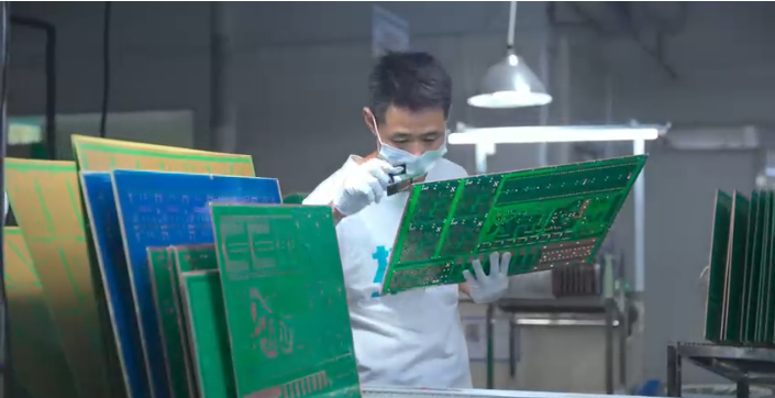
Introduction
In the intricate world of Printed Circuit Board (PCB) fabrication, perfection is often a moving target. While manufacturers frequently battle common defects—such as pinholes, uneven coating, or poor via plugging—there is one subtle yet critical factor that can drastically affect SMT soldering quality: solder mask misalignment.
Also known as registration error, this issue becomes increasingly volatile as electronic devices, like smartphones, demand smaller component sizes and denser layouts. While a minor shift might have been acceptable in the era of through-hole components, modern fine-pitch designs leave little room for error.
In this guide, we will explore what solder mask misalignment is, why it threatens product reliability, and how a combination of precise manufacturing at AIVON and smart design choices can prevent it.
Understanding Solder Mask Misalignment
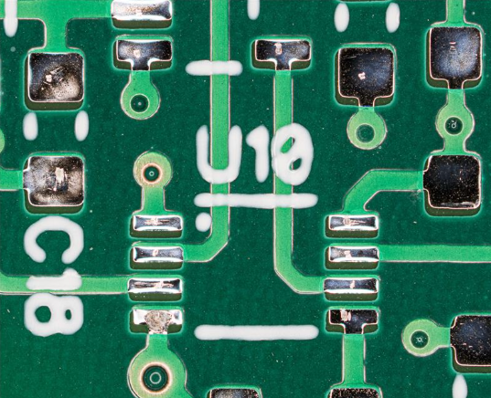
Solder mask misalignment refers to a positional error where the openings in the solder mask layer (the protective, usually green, ink) do not align perfectly with the copper pads they are meant to expose.
Ideally, the solder mask opening is designed to be slightly larger than the copper pad, creating a uniform "frame" of clearance around it. When misalignment occurs, this frame becomes lopsided; the mask may encroach on one side of the pad while leaving an excessive gap on the opposite side.
Industry Standards (IPC Acceptance Criteria)
It is important to note that absolute perfection is impossible in mass production. According to industry standards IPC-A-600H and IPC-6012E, a certain degree of shift is permissible.
For Class 2 products (most consumer and industrial electronics), the criteria generally state:
- The solder mask must not encroach onto the pad by more than 20% of the pad area or 1 mil (≈25.4 µm), whichever is greater.
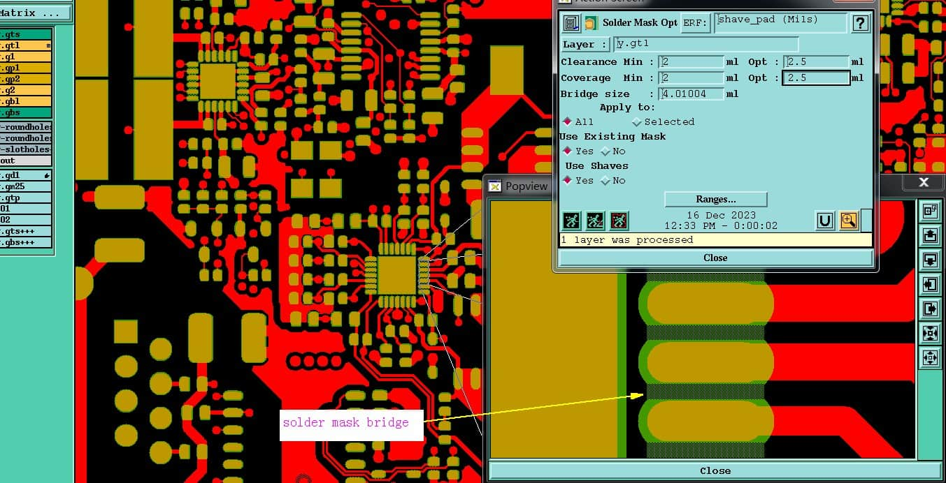
- The misalignment must not compromise the solder mask dam (the bridge of ink between pads) to the point where the minimum dam width is violated.
The Negative Impacts on Assembly and Reliability
Solder mask misalignment is not merely a cosmetic blemish; it is a functional defect that directly impacts manufacturing yield and long-term product life.
Poor Pad Solderability
When the solder mask shifts and covers a portion of the pad intended for soldering, the effective surface area is reduced. This can lead to insufficient wetting during the reflow process, resulting in weak mechanical bonds or "cold joints."
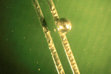
Solder Balls and Bridging
Misalignment often exposes copper circuitry that should be insulated. During the reflow soldering process, stray solder paste can flow onto these unintentionally exposed areas. This migration often results in the formation of loose solder balls or, worse, solder bridging (shorts) between fine-pitch leads.
Solder Mask Dam Failure
The solder mask dam is the physical barrier that prevents solder from flowing between two adjacent pads. A significant registration error can narrow or completely eliminate this dam. Without this barrier, the risk of solder bridging increases exponentially.
Component Assembly Issues
For advanced components like fine-pitch BGAs (Ball Grid Arrays) or CSPs (Chip Scale Packages), mask encroachment impacts the coplanarity of solder balls. This unevenness can cause open circuits or create localized stress points after the solder cools.
Long-Term Reliability Risks
Even if a board passes initial testing, hidden defects like stress concentration points or weak joints are susceptible to failure under thermal cycling or vibration, significantly shortening the product's lifespan.
Related Reading: Solder Mask Misalignment: Causes, Consequences, and Solutions for Robust PCB Production
Root Causes of Solder Mask Misalignment
Understanding the "why" behind misalignment requires looking at both the manufacturing floor and the design desk.
From the Manufacturing Perspective
- Exposure Registration Accuracy: The primary cause is often the alignment system used during UV exposure. If the optical alignment between the phototool (film) and the PCB is imprecise, or if the operator is inexperienced, the entire mask layer will shift.
- Phototool Deformation: Traditional film phototools are sensitive to temperature and humidity. According to IPC-A-600G, linear expansion tolerances can range from 1 to 2.5 mil per inch. Even a microscopic expansion in the film can lead to significant offsets on a large panel.
- Material Movement: PCB core materials (like FR-4) expand and contract during high-temperature processes like lamination and drilling. If the manufacturer does not calculate compensation factors for this movement, the mask will not line up with the copper pattern.
- Process Uniformity: Uneven solder mask coating or excessive pre-baking can cause local distortions. Furthermore, aggressive developing speeds can fail to clear the mask residue from pads, simulating the effect of misalignment.
From the PCB Design Perspective
- Inadequate Opening Ratios: If the clearance between the mask opening and the pad is too tight (e.g., 1:1 ratio), even standard manufacturing tolerances will result in encroachment.
- Narrow Dams: Designing dams that are too thin leaves no margin for error. A slight shift can cause the dam to vanish, leading to bridging.
- Asymmetric Layouts: Large, unbalanced copper areas can cause the board to warp or stretch unevenly during fabrication. This non-linear deformation is extremely difficult for manufacturers to compensate for globally.
AIVON Solutions
To combat these challenges, leading manufacturers like AIVON employ strict process controls and advanced technology to ensure registration accuracy.
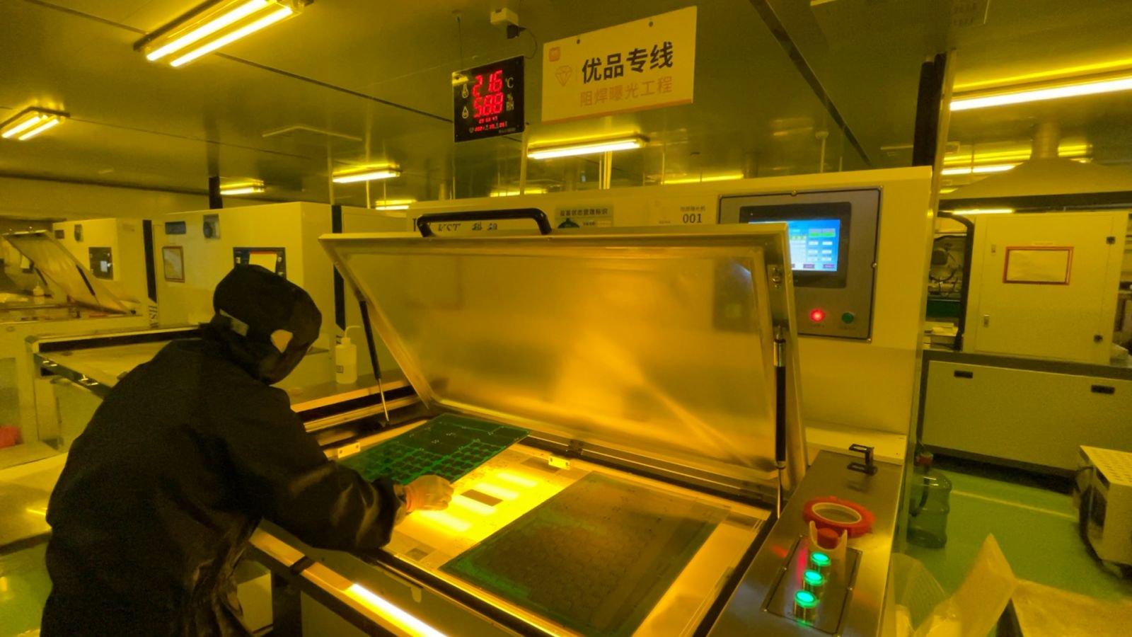
- Laser Direct Imaging (LDI): Where applicable, LDI replaces traditional film exposure. By writing the image directly onto the board using digital data, LDI eliminates phototool deformation and can dynamically scale the image to match the actual board dimensions.
- Environmental Controls: The CAM department and production floor maintain strict temperature and humidity levels to minimize the expansion or contraction of films and panels.
- Pre-Production Verification:
- Tooling Check: Operators verify alignment holes and use magnification to check BGA and inner-layer alignment (typically maintaining accuracy within 1.5–2 mil).
- Phototool Inspection: Before exposure, films are checked against the PCB. If deformation is detected, the film is scrapped and regenerated.
- First-Article Inspection: Developing parameters are validated on a "first article" board. Mass production only begins once the shift leader confirms that the mask development is clean and accurate.
Design Guidelines for Optimization
While manufacturers control the process, designers control the input. By optimizing your design data, you can create a "safety net" that accommodates natural manufacturing tolerances.
Solder Mask Opening vs. Pad Size
Always design the solder mask opening to be larger than the copper pad.
- General Rule: Pad Size + 0.1 mm (approx. 4 mil) overall.
- Per Side: Pad Size + 0.05 mm (approx. 2 mil) per side.
| Feature Type | Recommended Expansion | Note |
|---|---|---|
| Standard Components | 3–4 mil (75–100 µm) | Best for yield and cost efficiency. |
| High-Density / Fine-Pitch | 1–2 mil (25–50 µm) | Consult Manufacturer first. Requires tight process control. |
Solder Mask Dam Width
Ensure your design leaves enough space for a viable dam.
- Standard Designs: ≥ 4 mil (100 µm)
- High-Density Designs: ≥ 3 mil (75 µm)
If space is extremely limited, consult your manufacturer about using NSMD (Non-Solder Mask Defined) vs. SMD (Solder Mask Defined) pads, as their tolerance behaviors differ.
Related Reading: Optimizing Solder Mask Design for 4 Layer PCBs: Enhancing Reliability and Manufacturability
Clear Communication
Finally, ensure your Gerber files clearly distinguish between mask and pad layers. Always conduct a Design for Manufacturing (DFM) review with AIVON engineers before production to confirm that your layout aligns with factory capabilities.
FAQs
Q1: What is solder mask misalignment in PCB manufacturing?
A1: Solder mask misalignment occurs when solder mask openings do not accurately align with PCB pads. This can cause partial pad coverage or exposed copper, negatively affecting solderability, SMT assembly quality, and overall PCB reliability, especially on fine-pitch and high-density designs.
Q2: How does solder mask misalignment affect SMT soldering quality?
A2: Solder mask misalignment can reduce effective pad area, weaken solder joints, and eliminate solder mask dams. These issues often lead to solder bridging, solder balls, cold joints, and open circuits, significantly lowering assembly yield and long-term product reliability.
Q3: How can solder mask misalignment be prevented in PCB design and fabrication?
A3: Proper solder mask expansion, sufficient solder mask dam width, accurate layer alignment, and balanced copper distribution help minimize misalignment. Additionally, close DFM communication with the PCB manufacturer and strict process control during exposure and development are essential for consistent results.


