Introduction
In the fast-evolving field of electronics, the demand for compact, efficient, and high-performing devices drives innovation in printed circuit board (PCB) design. High-density interconnect (HDI) technology has emerged as a critical solution to meet these needs, with stacked microvias playing a pivotal role. These tiny vertical interconnects allow engineers to create intricate multilayer boards with fine-line routing, supporting advanced applications in telecommunications, medical devices, and consumer electronics. By enabling tighter component placement and enhanced signal integrity, stacked microvias address the challenges of miniaturization without compromising reliability. This article explores the technical foundations of microvias in HDI PCB design, their benefits, and best practices for implementation. Aimed at electrical engineers, the discussion provides a detailed look into how this technology shapes modern electronics.
What Are Stacked Microvias and Why Do They Matter?
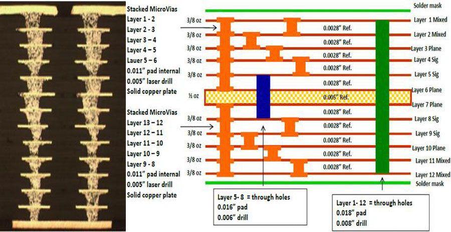
Stacked microvias are small, laser-drilled holes in a PCB that connect multiple layers in a vertical stack, unlike traditional staggered vias that are offset across layers. Typically measuring less than 0.15 mm in diameter, microvias facilitate high-density interconnects by allowing more connections in a smaller footprint. In HDI PCB designs, they are often used in blind or buried configurations, meaning they do not pass through the entire board thickness. This structure frees up surface space for fine-line routing and dense component layouts.
Their importance lies in enabling miniaturization and performance. As devices shrink, traditional through-hole vias become impractical due to size constraints. Stacked microvias support the integration of complex circuits in limited space, crucial for applications like smartphones and wearable technology. Additionally, they improve signal integrity by reducing parasitic effects, a key concern in high-speed designs. For engineers, understanding microvias is essential to meet the demands of next-generation electronics.
Technical Principles of Stacked Microvias in HDI PCB Design
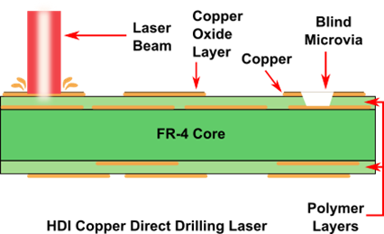
The functionality of stacked microvias relies on precise engineering and manufacturing processes. These vias are created using laser drilling, which offers accuracy for small diameters and aspect ratios. In a typical HDI PCB, microvias connect adjacent layers, often stacked directly on top of each other to form a continuous vertical path. This contrasts with staggered vias, where connections are offset, requiring more board space.
The design of stacked microvias must account for aspect ratio, defined as the depth-to-diameter ratio of the via. A common guideline, as outlined in industry standards like IPC-2226, is to maintain an aspect ratio below 1:1 to ensure reliable plating and filling. Higher ratios can lead to voids or incomplete copper deposition, risking electrical failure. Materials also play a role, with dielectric layers needing to withstand laser drilling without excessive charring or delamination.
Signal integrity benefits from stacked microvias due to shorter interconnect lengths. In high-speed designs, this reduces inductance and crosstalk, critical for maintaining data rates. However, thermal and mechanical stresses during fabrication can challenge via reliability, necessitating strict adherence to design rules and process controls.
Related Reading: Microvia PCB Design Rules: A Practical Handbook for Error Free HDI Layouts

Benefits of Stacked Microvias for High-Density Interconnects
Stacked microvias offer several advantages in HDI PCB design, making them indispensable for advanced electronics. First, they enable significant space savings. By connecting layers vertically without lateral offsets, they allow for tighter trace routing and higher component density. This is vital for compact devices where every square millimeter counts.
Second, they enhance electrical performance. The reduced path length minimizes signal loss and interference, supporting high-frequency applications. For instance, in 5G hardware, microvias help maintain signal clarity over dense interconnects. Third, they support complex multilayer stackups, often exceeding ten layers, without increasing board thickness excessively.
Finally, stacked microvias improve thermal management. Their small size and direct paths allow heat dissipation across layers, reducing hotspots in dense designs. For engineers, these benefits translate to greater design flexibility and reliability, aligning with the needs of modern electronics.
Challenges in Implementing Stacked Microvias
While stacked microvias are transformative, they present distinct challenges. Fabrication complexity is a primary concern. Laser drilling requires precision to avoid damaging surrounding materials, and stacking multiple microvias increases the risk of misalignment. Standards such as IPC-6012E emphasize the need for tight process controls during manufacturing to ensure via integrity.
Reliability under thermal stress is another issue. Repeated temperature cycles, as seen in reflow soldering, can cause microvia cracking or separation if not designed properly. Adherence to guidelines in IPC-A-600K for acceptability criteria helps mitigate such risks. Additionally, the cost of HDI PCB production with stacked microvias can be higher due to specialized equipment and materials.
Signal integrity, while improved, demands careful planning. Impedance mismatches at via transitions can occur if stackup geometry is not optimized. Engineers must balance these challenges with performance goals, often relying on simulation tools to predict outcomes before fabrication.
Best Practices for Designing with Stacked Microvias
To maximize the benefits of stacked microvias in HDI PCB design, engineers should follow established best practices. Start with thorough planning of the layer stackup. Define via locations early to ensure alignment with fine-line routing requirements. Standards like IPC-2226 provide detailed guidance on HDI design, including via placement and spacing.
Maintain conservative aspect ratios for microvias. Keeping depth-to-diameter ratios low ensures reliable copper plating and reduces failure risks. Use simulation software to analyze signal integrity, focusing on impedance control across via transitions. This is especially important for high-speed designs where even minor deviations impact performance.
Select appropriate materials for dielectric layers. High-frequency laminates with low dielectric loss support microvia formation and signal transmission. During manufacturing, ensure compliance with IPC-6012E for performance specifications, verifying that vias meet dimensional and structural criteria. Regular inspection, guided by IPC-A-600K, helps identify defects like voids or cracks before they cause issues.
Collaboration between design and manufacturing teams is critical. Early feedback on process capabilities prevents design choices that are difficult to fabricate. By integrating these practices, engineers can achieve robust HDI PCB designs with stacked microvias.
Practical Applications of Stacked Microvias in Advanced Electronics
Stacked microvias find extensive use in various high-density applications. In telecommunications, they enable compact base station hardware with multilayer boards supporting high-speed data transfer. Medical devices, such as imaging equipment, rely on microvias for dense interconnects within limited enclosures, ensuring reliable operation.
Consumer electronics, particularly smartphones and tablets, benefit immensely. These devices pack numerous components into thin profiles, made possible by HDI PCB technology with stacked vias. Automotive systems also adopt microvias for advanced driver assistance systems, where space and reliability are non-negotiable.
In each application, the ability to route fine lines and stack multiple layers without increasing board size is a game-changer. Engineers must tailor designs to specific use cases, balancing density with thermal and electrical constraints. The versatility of stacked microvias continues to open new possibilities across industries.
Related Reading: Microvia PCB for RF Applications: Design Considerations for High Frequency Performance
Conclusion
Stacked microvias stand at the forefront of HDI PCB technology, enabling high-density interconnects essential for advanced electronics. Their ability to save space, enhance signal integrity, and support complex multilayer designs addresses the pressing needs of miniaturization and performance. While challenges like fabrication complexity and thermal reliability exist, adherence to industry standards and best practices ensures successful implementation. For electrical engineers, mastering the use of microvias in PCB design unlocks the potential to innovate across telecommunications, medical, and consumer applications. As technology advances, the role of stacked microvias will only grow, shaping the future of compact, high-speed electronics.
FAQs
Q1: What are stacked microvias, and how do they differ from staggered vias in HDI PCB design?
A1: Stacked microvias are small, vertically aligned holes connecting multiple layers directly on top of each other in an HDI PCB. Unlike staggered vias, which are offset across layers and consume more space, stacked microvias enable tighter layouts and fine-line routing. This makes them ideal for compact, high-density designs where space is limited, though they require precise fabrication to ensure reliability.
Q2: How do stacked microvias improve signal integrity in high-density interconnects?
A2: Stacked microvias enhance signal integrity in HDI PCB designs by shortening interconnect paths, reducing inductance and crosstalk. Their small size minimizes parasitic effects, which is critical for high-speed applications. By enabling precise fine-line routing, they help maintain consistent impedance, ensuring clear signal transmission in dense layouts like those found in modern telecommunications hardware.
Q3: What standards guide the design of microvias in HDI PCB layouts?
A3: Industry standards such as IPC-2226 for HDI design, IPC-6012E for performance specifications, and IPC-A-600K for acceptability criteria are essential for microvia implementation. These guidelines cover aspect ratios, via placement, and inspection requirements to ensure structural integrity and electrical performance. Following them helps engineers avoid common issues during fabrication of high-density boards.
Q4: What challenges should engineers anticipate with stacked microvias in PCB design?
A4: Engineers face challenges like fabrication precision, thermal stress reliability, and higher production costs with stacked microvias in HDI PCB design. Misalignment during laser drilling or cracking under temperature cycles can compromise performance. Strict adherence to design rules and process controls, as outlined in relevant standards, is necessary to mitigate these risks effectively.
References
IPC-2226 - Design Standard for High Density Interconnect (HDI) Printed Boards. IPC, 2017.
IPC-6012E - Qualification and Performance Specification for Rigid Printed Boards. IPC, 2020.
IPC-A-600K - Acceptability of Printed Boards. IPC, 2020.


