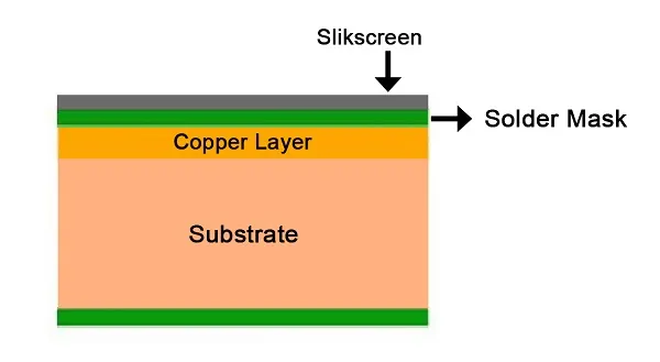
Introduction
In the realm of printed circuit board (PCB) design, achieving optimal routing for Ball Grid Array (BGA) components is a critical challenge for electrical engineers. As component density increases and board real estate shrinks, the choice of via technology becomes pivotal. Two prominent solutions, stacked via and via-in-pad, offer distinct approaches to managing high-density interconnects (HDI) in PCB layouts. These technologies address the complexities of BGA routing by enabling efficient signal paths and component placement while adhering to the demands of modern electronics. This article explores the technical underpinnings of stacked vias and via-in-pad designs, compares their applications in HDI PCB contexts, and provides practical guidance for engineers. By understanding their strengths and limitations, designers can make informed decisions to enhance performance and reliability in their projects.
What Are Stacked Vias and Via-in-Pad Technologies?
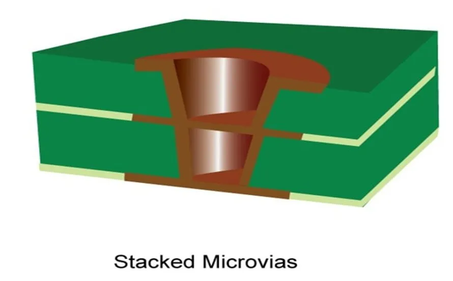
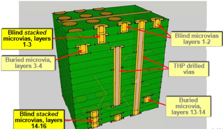
Both stacked vias and via-in-pad technologies are integral to HDI PCB design, particularly for BGA routing where space constraints and signal integrity are paramount. Stacked vias refer to a configuration where multiple vias are vertically aligned across different layers of a multilayer PCB, often using microvias to connect adjacent layers. This method is common in high-density designs to minimize the footprint and facilitate intricate routing.
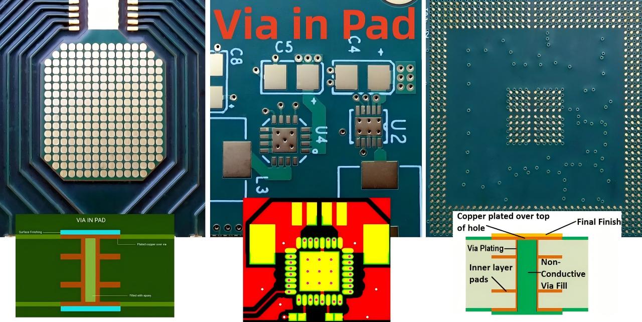
Via-in-pad, on the other hand, involves placing a via directly within the pad of a surface-mount component, such as a BGA. This approach reduces the need for additional routing space by integrating the via into the component's landing area, thereby optimizing board space. Both technologies aim to solve challenges in component placement and routing density, but they cater to different design needs and manufacturing constraints. Their relevance in modern PCB design lies in enabling smaller, faster, and more reliable electronic devices.
Related Reading: Stacked Vias in HDI PCBs: Design, Manufacturing, and Reliability
Technical Principles of Stacked Vias and Via-in-Pad
Stacked Vias in HDI PCB Design
Stacked vias are a cornerstone of HDI PCB technology, allowing engineers to connect multiple layers in a compact manner. Typically, microvias, which are small-diameter vias created using laser drilling, are stacked on top of each other to form a continuous vertical path. This setup is governed by standards such as IPC-2226, which outlines design considerations for HDI structures. Stacked vias minimize the lateral space required for routing, making them ideal for fine-pitch BGA components where pin density is high.
The primary advantage of stacked vias is their ability to support complex multilayer designs without increasing the board's footprint. However, they require precise manufacturing processes to ensure alignment and reliability across layers. Misalignment or defects in drilling can lead to signal integrity issues or structural weaknesses. Engineers must also consider the aspect ratio of microvias to prevent fabrication challenges, as specified in IPC-6012E for rigid printed boards.
Via-in-Pad for BGA Routing
Via-in-pad technology involves placing a via directly under the pad of a BGA or other surface-mount component. This design is particularly useful for fine-pitch BGAs, where traditional routing methods consume excessive space. By embedding the via within the pad, designers can route signals directly from the component to inner layers without detouring traces around the pad area. This approach aligns with guidelines in IPC-A-600K for acceptable printed board designs.
The via-in-pad method often requires filling the via with conductive or non-conductive material to prevent solder wicking during assembly, a process detailed in standards like IPC-4761 for via protection. While this technology maximizes space efficiency, it introduces manufacturing complexities, such as ensuring proper via filling and maintaining pad flatness for reliable soldering. Signal integrity can also be affected if the via impacts the pad's contact area or if impedance mismatches occur.
Key Differences in Application
Stacked vias and via-in-pad serve overlapping yet distinct purposes in BGA routing. Stacked vias excel in multilayer HDI PCB designs where vertical interconnects are critical for connecting numerous layers. They are less intrusive to surface component placement but demand advanced fabrication techniques. Via-in-pad, conversely, directly addresses surface space constraints by integrating vias into pads, though it may complicate assembly and require additional process steps. Understanding these principles helps engineers select the appropriate technology based on design goals and manufacturing capabilities.
Practical Applications and Best Practices for BGA Routing
When to Use Stacked Vias
Stacked vias are best suited for HDI PCB designs with high layer counts and dense BGA components. They are particularly effective in applications like telecommunications and computing devices, where signal layers must be interconnected without sacrificing board space. To implement stacked vias effectively, engineers should adhere to design rules outlined in IPC-2226, such as maintaining appropriate via aspect ratios and ensuring layer-to-layer registration accuracy during fabrication.
A key best practice is to limit the number of stacked microvias to avoid reliability issues. Overstacking can lead to mechanical stress or thermal expansion mismatches, impacting long-term performance. Designers should also collaborate with fabricators to confirm process capabilities, as not all facilities support high-precision microvia stacking. Simulation tools can aid in predicting signal integrity and identifying potential bottlenecks before manufacturing begins.
When to Use Via-in-Pad
Via-in-pad is ideal for designs where board space is at a premium and fine-pitch BGA components dominate the layout. This technology shines in compact consumer electronics, such as smartphones and wearables, by allowing direct routing beneath components. However, implementing via-in-pad requires careful consideration of assembly processes. Standards like IPC-4761 recommend via filling to prevent solder escape, which can compromise joint reliability.
Engineers should specify whether conductive or non-conductive fill is needed based on thermal and electrical requirements. Additionally, pad design must ensure sufficient contact area for soldering, avoiding interference from the via. Close coordination with assembly teams is essential to confirm that reflow profiles and stencil designs accommodate via-in-pad structures without defects.
Balancing Component Placement and Routing Density
Effective BGA routing hinges on balancing component placement with via technology selection. Stacked vias allow greater flexibility in placing components across layers, as they do not occupy surface pad space. However, they may necessitate additional layers, increasing cost. Via-in-pad conserves surface area but can restrict placement options if not planned carefully. Designers must evaluate signal paths, power distribution, and thermal management when deciding between these approaches. Following IPC-A-600K guidelines for acceptability ensures that the chosen method aligns with quality expectations.
Comparative Analysis: Stacked Via vs. Via-in-Pad for HDI PCB
- Space Efficiency: Stacked Via - High for multilayer routing; Via-in-Pad - High for surface component density.
- Manufacturing Complexity: Stacked Via - Requires precise microvia alignment; Via-in-Pad - Needs via filling and pad optimization.
- Signal Integrity: Stacked Via - Better for complex layer transitions; Via-in-Pad - Potential impedance issues if unfilled or poorly implemented.
- Cost Impact: Stacked Via - Higher due to HDI processes; Via-in-Pad - Moderate, depends on fill material and assembly steps.
- Best Use Case: Stacked Via - Multilayer HDI PCB with dense routing; Via-in-Pad - Fine-pitch BGA in compact designs.
This comparison highlights the trade-offs between stacked vias and via-in-pad. Stacked vias are preferable for intricate multilayer designs, while via-in-pad suits surface-constrained layouts. Engineers must weigh these factors against project requirements, such as performance and budget, to determine the optimal approach.
Troubleshooting Common Issues in BGA Routing
In stacked via designs, a common issue is via misalignment during fabrication, which can disrupt signal paths. Engineers should verify fabricator capabilities and request adherence to IPC-6012E standards for qualification and performance. Regular inspection of via stack integrity using cross-sectional analysis can identify defects early.
For via-in-pad, solder wicking into unfilled vias often poses challenges during assembly. Specifying appropriate via protection methods, as per IPC-4761, mitigates this risk. Additionally, thermal stress from reflow can affect pad adhesion if via filling is uneven. Testing under controlled conditions, following IPC-A-600K acceptability criteria, ensures consistent results. Addressing these issues upfront streamlines the design-to-manufacturing transition for both technologies.
Related Reading: Troubleshooting Common Via-in-Pad Issues in PCB Design
Conclusion
Selecting between stacked via and via-in-pad technologies for BGA routing in PCB design requires a thorough understanding of project constraints and performance goals. Stacked vias offer robust solutions for multilayer HDI PCB layouts, supporting complex routing with minimal surface impact. Via-in-pad excels in maximizing board space for fine-pitch components, though it demands careful assembly planning. By aligning design choices with standards like IPC-2226 and IPC-4761, electrical engineers can optimize component placement and signal integrity. Ultimately, the best choice depends on balancing space, cost, and manufacturing capabilities to achieve reliable, high-performance designs tailored to specific applications.
FAQs
Q1: What are the main advantages of stacked vias in HDI PCB design?
A1: Stacked vias provide significant space savings in multilayer HDI PCB designs by enabling vertical interconnects with microvias. They support dense BGA routing without consuming surface area, making them ideal for complex, high-layer-count boards. Following standards like IPC-2226 ensures reliable implementation. Their ability to connect multiple layers efficiently enhances signal integrity in demanding applications.
Q2: How does via-in-pad technology improve BGA routing efficiency?
A2: Via-in-pad technology optimizes BGA routing by placing vias directly under component pads, reducing the need for additional trace space. This approach is critical for fine-pitch BGAs in compact designs. It enhances component placement density on the surface layer. Adhering to IPC-4761 for via protection ensures assembly reliability, making it a practical choice for space-constrained projects.
Q3: What challenges arise with via-in-pad in PCB design?
A3: Via-in-pad in PCB design can introduce assembly challenges, such as solder wicking into unfilled vias, impacting joint reliability. It requires via filling and precise pad design to maintain contact integrity. Manufacturing complexity increases due to additional process steps. Following IPC-A-600K guidelines helps address acceptability concerns, ensuring consistent performance during production.
Q4: When should engineers prioritize stacked vias over via-in-pad for BGA routing?
A4: Engineers should prioritize stacked vias for BGA routing in multilayer HDI PCB designs where vertical interconnects are essential. They suit projects with high layer counts and complex signal paths. Stacked vias avoid surface pad interference, enhancing component placement flexibility. Standards like IPC-6012E guide reliable fabrication, making them preferable for intricate routing needs.
References
IPC-2226 - Design Standard for High Density Interconnect (HDI) Printed Boards. IPC, 2003.
IPC-6012E - Qualification and Performance Specification for Rigid Printed Boards. IPC, 2020.
IPC-A-600K - Acceptability of Printed Boards. IPC, 2020.
IPC-4761 - Design Guide for Protection of Printed Board Via Structures. IPC, 2006.