Introduction
The relentless progression of electronic technology, marked by increasing data rates, higher operating frequencies, and sophisticated wireless communication, places unprecedented demands on printed circuit board (PCB) design. At the core of achieving reliable performance in these advanced systems lies the strategic design of the PCB stackup. A well-engineered stackup is paramount for controlling signal integrity, minimizing electromagnetic interference (EMI), and ensuring consistent impedance. This guide, presented by AIVON, will explore the fundamental principles of stackup design and underscore the critical importance of material selection when developing PCBs for high-frequency applications, moving beyond the limitations of conventional FR-4.
What is a PCB Stackup and Why Material Selection Matters for High Frequency?
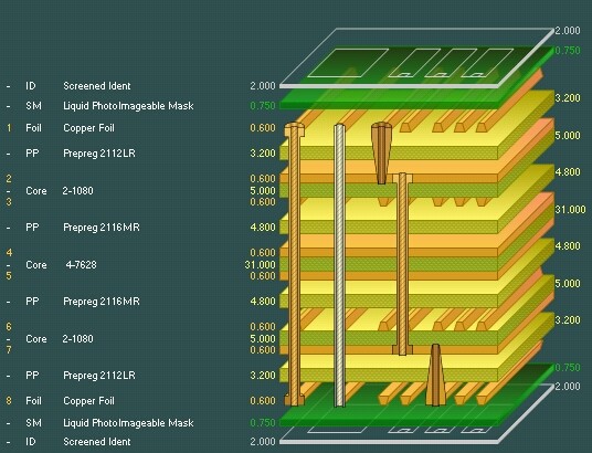
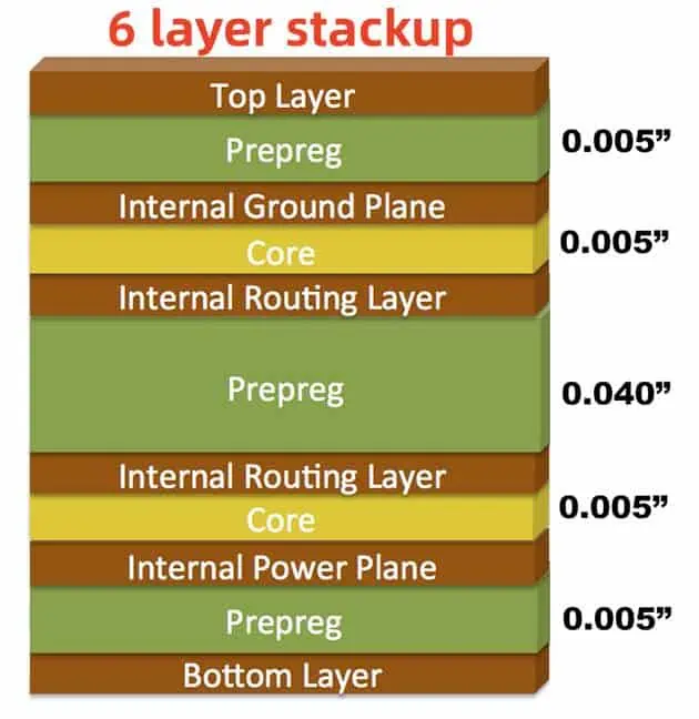
A PCB stackup refers to the arrangement of conductive copper layers and insulating dielectric materials that make up the printed circuit board. It is essentially a layered cake of copper traces, ground planes, power planes, and dielectric laminates. The design of this layered structure profoundly influences the electrical characteristics of signals propagating through the board.
For high-frequency applications, the choice of material selection within the stackup becomes exceptionally critical because signals behave differently as their frequencies increase. At higher frequencies, PCB traces act as transmission lines, where signal integrity is highly sensitive to the properties of the surrounding dielectric materials. Improper material selection can lead to significant signal degradation, including:
- Impedance Mismatches: Causing signal reflections and reducing effective power transfer.
- Signal Loss (Attenuation): Weakening the signal over distance due to energy absorption by the dielectric.
- Crosstalk: Unwanted coupling of signals between adjacent traces.
- Electromagnetic Interference (EMI): Increased radiation or susceptibility due to uncontrolled electromagnetic fields.
Therefore, meticulous material selection in the stackup is not merely a preference but a necessity for meeting the stringent performance requirements of modern high-frequency electronics.
Key Material Properties for High-Frequency Stackups
When designing for high-frequency performance, several key material properties of the dielectric laminates must be carefully evaluated. These properties directly influence signal behavior and overall circuit reliability.
1. Dielectric Constant (Dk or Er)
The dielectric constant (Dk) is a fundamental measure of a material's ability to store electrical energy within an electric field.
- Low and Stable Dk: For high-frequency applications, a low and stable Dk is crucial. A low Dk ensures faster signal propagation speeds, as signals travel faster through materials with lower Dk values.
- Consistency: Stability of Dk with varying frequency, temperature, and moisture absorption is vital. Any significant change in Dk can alter the characteristic impedance of transmission lines, leading to signal reflections and degradation. Precise impedance control, essential for high-frequency designs, relies heavily on a consistent Dk. IPC-4101E, Specification for Base Materials for Rigid and Multilayer Printed Boards, categorizes materials and their Dk values.
2. Dissipation Factor (Df or tan δ)
The dissipation factor (Df), also known as loss tangent, quantifies the energy loss within a dielectric material as a signal propagates through it.
- Low Df: A low Df is paramount for minimizing signal loss (attenuation) in high-frequency circuits. High Df materials absorb more signal energy, converting it into heat and reducing the signal's amplitude. This is particularly critical for long transmission lines or high-power applications.
- Frequency Dependence: The Df should remain low and stable across the operating frequency range to maintain signal strength and power efficiency.
3. Coefficient of Thermal Expansion (CTE)
The Coefficient of Thermal Expansion (CTE) describes how much a material expands or contracts in response to temperature changes.
- Z-Axis CTE Match: For multi-layer PCBs, the CTE in the z-axis (thickness direction) is particularly important. A CTE mismatch between the dielectric material and the copper plating in plated through-holes (PTHs) can induce significant stress during thermal cycling. This stress can lead to barrel cracks in the PTHs or delamination, compromising reliability. Materials with a CTE that closely matches copper's CTE (approximately 17 ppm/°C) are preferred.
- X/Y-Axis CTE: A low and stable CTE in the x and y axes (planar directions) contributes to the dimensional stability of the PCB, which is important for precise component placement and alignment in dense designs.
4. Moisture Absorption
Moisture absorption refers to the amount of water a material absorbs from the environment.
- Low Moisture Absorption: High-frequency laminates should have very low moisture absorption. Water molecules possess a relatively high Dk and Df. Even small amounts of absorbed moisture can significantly alter the electrical properties (Dk and Df) of the dielectric material, leading to unpredictable circuit performance and increased signal loss, especially in humid conditions.
Common High-Frequency Stackup Materials (Beyond FR-4)
While FR-4 has been the industry standard for many years, its inherent limitations in Df (typically 0.018-0.025 at 1 GHz) and variable Dk (typically 4.2-4.7) make it increasingly unsuitable for demanding high-frequency applications. Specialized advanced PCB laminates are required to meet modern performance specifications.
1. Hydrocarbon Resin / Ceramic-Filled Laminates (e.g., Rogers RO4000 Series)
These materials combine hydrocarbon resins with ceramic fillers to achieve a balance of electrical performance, thermal stability, and processability.
- Properties: They offer low and stable Dk values (e.g., 2.55 to 6.15) and significantly lower Df values (e.g., 0.002 to 0.004) compared to FR-4. They also have improved z-axis CTE, making them more reliable for multi-layer structures. Many of these materials are designed to be processed using standard FR-4 manufacturing techniques, which can ease integration into existing production lines.
- Examples:
- RO4003C™ Laminates: Dk 3.38, Df 0.0027 at 10 GHz. Offers excellent electrical performance and processability, suitable for many RF applications like cellular base stations and power amplifiers.
- RO4350B™ Laminates: Dk 3.48, Df 0.0037 at 10 GHz. Provides similar performance to RO4003C but with slightly better power handling and thermal reliability, ideal for high-power RF front-ends.
- Applications: Widely used in automotive radar, cellular infrastructure, RF identification (RFID), and satellite communication systems.
Related Reading: Ceramic PCB vs. FR-4: Choosing the Right Material for Your High-Frequency Design
2. PTFE-based Laminates (e.g., Rogers RT/duroid Series)
Polytetrafluoroethylene (PTFE) based laminates are renowned for their extremely low electrical loss properties.
- Properties: They boast ultra-low Dk values (e.g., 2.20 to 3.50) and exceptionally low Df values (e.g., 0.0009 to 0.002). These properties ensure minimal signal attenuation and excellent signal integrity, particularly at millimeter-wave frequencies. PTFE materials also exhibit very low moisture absorption.
- Examples:
- RT/duroid® 5880 Laminates: Dk 2.20, Df 0.0009 at 10 GHz. Considered a benchmark for ultra-low loss, ideal for extremely high-frequency applications where signal attenuation must be minimized.
- RT/duroid® 6002 Laminates: Dk 2.94, Df 0.0012 at 10 GHz. Offers excellent Dk uniformity and stability, suitable for complex microwave circuits.
- Challenges: PTFE materials typically require specialized PCB manufacturing processes due to their inherent softness and ductility, which can increase fabrication costs.
- Applications: Critical for aerospace and defense (radar, electronic warfare), satellite systems, millimeter-wave applications, and high-frequency test and measurement equipment.
3. Thermoset Hydrocarbon Resins (e.g., Isola I-Terra, Panasonic Megtron Series)
These advanced thermoset materials offer excellent high-frequency performance with good thermal and mechanical properties.
- Properties: They feature low Dk and Df values, often comparable to or exceeding the performance of some ceramic-filled materials. They also provide good thermal reliability and processability, making them suitable for high-layer count designs.
- Examples:
- Isola I-Tera MT40: Known for low loss and good thermal reliability.
- Panasonic Megtron 6/7/8: Popular for high-speed digital and RF applications due to very low Df and stable Dk.
- Applications: Used in high-speed computing, network infrastructure, data centers, and advanced consumer electronics where both high-frequency performance and signal integrity for complex digital signals are critical.
Designing the High-Frequency Stackup: Practical Considerations
Effective stackup design for high-frequency applications goes beyond simply choosing materials; it involves integrating these materials into a structure that optimizes electrical performance.
1. Impedance Control
- Consistent Dk and Thickness: Achieving precise impedance control for transmission lines (microstrips and striplines) relies heavily on the consistency of the dielectric layer's Dk and thickness. Variations can lead to signal reflections.
- Reference Planes: Solid, continuous ground and power planes are essential. They provide stable reference potentials and define the return current paths for high-frequency signals, which is critical for impedance control. IPC-2221A, Generic Standard on Printed Board Design, outlines general design principles for stackups.
2. Signal Integrity
- Crosstalk Minimization: Strategic placement of signal layers, adequate spacing between traces, and the use of guard traces or differential pairs help minimize unwanted signal coupling (crosstalk).
- EMI Reduction: Proper grounding, effective return path management, and the use of shield layers within the stackup are crucial for containing EMI and preventing interference with other electronic systems.
- Power Delivery Network (PDN) Noise: Designing a robust PDN with sufficient decoupling capacitors and low inductance planes is vital to ensure stable power delivery and minimize noise that can affect high-frequency signals.
3. Thermal Management Integration
While high-frequency materials primarily focus on electrical properties, their thermal conductivity also matters.
- Heat Spreading: Utilizing internal copper planes as heat spreaders helps distribute heat away from localized hot spots.
- Thermal Vias: Strategically placed thermal vias can provide low resistance thermal pathways from heat-generating components to ground planes or external heat sinks, leveraging the thermal conductivity of the copper and the dielectric.
4. Hybrid Stackups
For designs that combine high-frequency circuits with less critical digital or power sections, hybrid stackups are often employed.
- Cost Optimization: This approach uses premium high-frequency laminates only where necessary (e.g., for RF layers) and more cost-effective FR-4 for other layers.
- Challenges: Hybrid constructions require careful consideration of CTE mismatches between different materials during the lamination process to prevent warpage and maintain reliability. IPC-2223C, Sectional Design Standard for Flexible Printed Boards, includes considerations for rigid-flex hybrid structures, applicable in principle to mixed material rigid boards.
Related Reading: Mastering 12-Layer PCB Stackups for High-Performance High-Speed Designs
Manufacturing Considerations for Advanced Stackup Materials
The successful fabrication of PCBs with advanced PCB laminates requires specialized PCB manufacturing capabilities.
- Fabrication Capabilities: Manufacturers must possess the expertise and equipment for processing diverse materials, including precise drilling, specialized desmear processes (especially for PTFE), and controlled etching of fine features.
- Process Control: Tighter controls on dielectric thickness tolerances, copper etching, and lamination cycles are necessary to maintain the electrical characteristics of high-frequency laminates.
- Material Handling: Different laminates may have specific handling and storage requirements to prevent damage or moisture absorption. IPC-A-600K, Acceptability of Printed Boards, provides guidelines for acceptable board characteristics.
Conclusion
The strategic material selection for a PCB stackup is undeniably critical for the success of high-frequency applications. Moving beyond the limitations of FR-4 to specialized advanced PCB laminates from reputable suppliers is essential for achieving superior signal integrity, minimizing loss, and ensuring reliable performance. By carefully evaluating key material properties such as Dk, Df, CTE, and moisture absorption, designers can make informed choices that optimize electrical and thermal performance. AIVON emphasizes that combining the right materials with meticulous stackup design, stringent process control, and comprehensive manufacturing expertise is paramount for developing robust, high-performance, and cost-effective electronic systems for today's demanding technological landscape.
FAQs
Q1: Why is Dielectric Constant (Dk) stability crucial for high-frequency PCB stackups?
A1: Dielectric Constant (Dk) stability is crucial for high-frequency PCB stackups because variations in Dk can alter the characteristic impedance of transmission lines. This leads to signal reflections, degraded signal integrity, and unpredictable circuit performance across different frequencies or temperatures.
Q2: How do advanced PCB laminates improve signal integrity compared to FR-4 in high-frequency applications?
A2: Advanced PCB laminates improve signal integrity by offering lower and more stable Dissipation Factor (Df) and Dielectric Constant (Dk) values than FR-4. This significantly reduces signal loss (attenuation), minimizes phase distortion, and enables more precise impedance control for high-frequency signals.
Q3: What are hybrid stackups and when are they used for high-frequency designs?
A3: Hybrid stackups combine high-frequency laminates for critical RF or high-speed layers with more cost-effective FR-4 for non-critical digital or power layers. They are used to optimize costs while ensuring localized high-frequency performance where necessary in complex designs.
Q4: What industry standards guide material selection and design for PCB stackups?
A4: Industry standards like IPC-2221A, Generic Standard on Printed Board Design, provide general design principles. IPC-4101E, Specification for Base Materials for Rigid and Multilayer Printed Boards, categorizes and specifies requirements for various laminate materials, guiding material selection for PCB stackups.
References
IPC-2221A — Generic Standard on Printed Board Design. IPC, 2003.
IPC-2223C — Sectional Design Standard for Flexible Printed Boards. IPC, 2017.
IPC-4101E — Specification for Base Materials for Rigid and Multilayer Printed Boards. IPC, 2021.
IPC-A-600K — Acceptability of Printed Boards. IPC, 2020.


