Introduction
Printed circuit boards form the backbone of electronic systems, and their physical dimensions play a critical role in project success. Engineers often face the choice between standard PCB dimensions and custom options during the design phase. Standard dimensions align with established manufacturing practices, while custom ones offer tailored solutions for unique requirements. This decision impacts cost, production time, and performance. Understanding the trade-offs helps electric engineers optimize designs for reliability and efficiency. Balancing these factors ensures projects meet both technical and budgetary goals.
Defining Standard PCB Dimensions and Their Industry Relevance
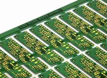
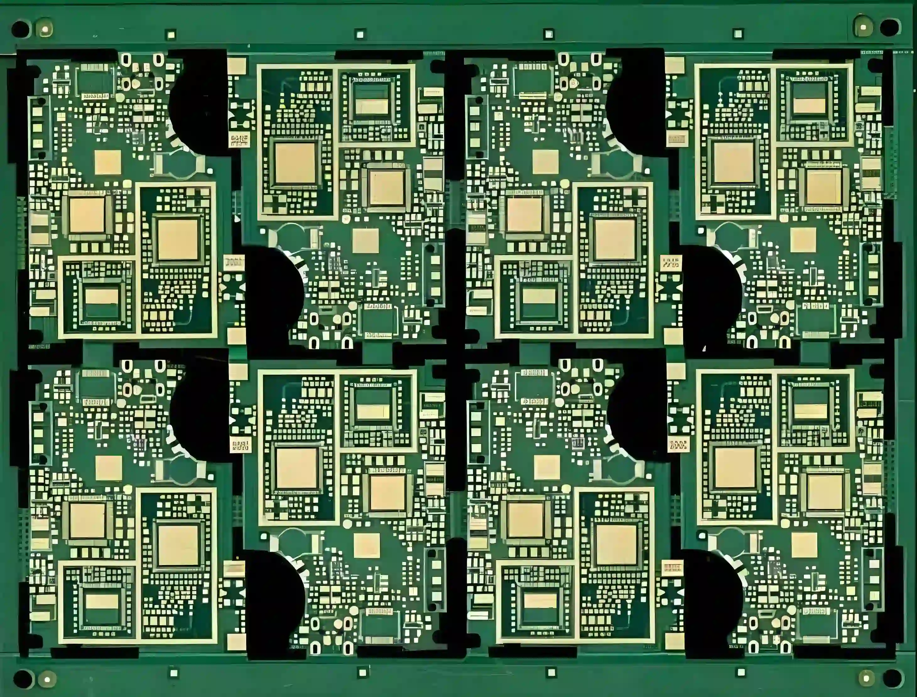
Standard PCB dimensions refer to sizes that fit efficiently within common fabrication panel formats, as guided by industry documents like IPC-D-322. These dimensions maximize material utilization during production, reducing waste and streamlining processes. Fabrication panels have predefined sizes that accommodate multiple boards, promoting consistency across high-volume runs. Electric engineers appreciate standard PCB dimensions applications in prototyping and production where speed matters. For instance, they suit rack-mounted systems or modular enclosures that follow conventional footprints. Deviating from these invites additional considerations in tooling and handling.
Standard sizes also simplify assembly and testing workflows. They align with automated equipment setups designed for uniform boards. This relevance extends to supply chain logistics, where standardized parts integrate seamlessly. However, relevance varies by project scale; low-volume designs may prioritize flexibility over conformity.
Technical Principles Behind Standard vs. Custom Dimensions
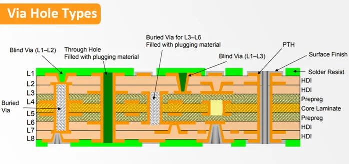
The principles governing PCB dimensions stem from material properties and manufacturing constraints. Standard dimensions minimize stress concentrations at edges, enhancing structural integrity under thermal cycling. IPC-2221 provides guidelines for board outlines, emphasizing clearances and rigidity to prevent warpage. Custom dimensions, while flexible, require precise control of aspect ratios to avoid fabrication defects like delamination. Engineers must evaluate signal integrity, as board size influences trace lengths and impedance matching.
Fabrication involves routing or scoring panels, where standard sizes optimize v-scoring paths. Custom shapes demand specialized tooling, potentially increasing annular ring stresses around vias. Dimensional stability ties to laminate CTE, affecting solder joint reliability in assembly. These mechanisms underscore why standard options excel in controlled environments.
Pros and Cons of Standard PCB Dimensions
Standard PCB dimensions offer clear advantages in cost and lead time. They leverage existing panel layouts, achieving higher yields and lower per-unit expenses. Production scales efficiently, ideal for standard PCB dimensions applications in consumer electronics or industrial controls. Turnaround times shorten due to familiar setups in etching and plating. Engineers benefit from predictable tolerances, aligning with IPC-6012 qualification specs for rigid boards.
However, limitations arise in design constraints. Standard sizes may force compromises in component placement or enclosure fit. PCB design flexibility suffers, potentially requiring workarounds like foldable sections. Overly rigid adherence can hinder innovation in compact or ergonomic products.
- Cost: Pros: Lower due to panel efficiency; Cons: None significant
- Lead Time: Pros: Faster prototyping; Cons: Limited to predefined sizes
- Yield: Pros: Higher material utilization; Cons: Less adaptable to unique needs
- Assembly: Pros: Compatible with standard fixtures; Cons: May not optimize space
Custom PCB Dimensions: Benefits and Challenges
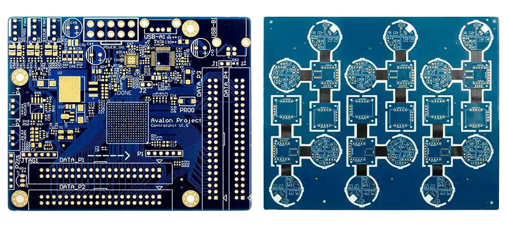
Custom PCB benefits shine in projects demanding precise fit, such as medical devices or aerospace modules. PCB design flexibility allows optimization for thermal dissipation or mechanical mounting. Engineers can incorporate non-rectangular outlines to match curved housings, improving system integration. These boards support advanced features like embedded stiffeners for vibration resistance.
Drawbacks center on non-standard PCB costs, driven by setup fees and material waste. Irregular dimensions reduce panel nesting efficiency, elevating expenses per board. Lead times extend for custom routing programs and inspections. Quality risks increase if tolerances stray from proven norms.
PCB Shape Considerations in Design Choices
PCB shape considerations profoundly affect manufacturability and performance. Rectangular forms dominate standard PCB dimensions applications for their simplicity in handling and fixturing. They facilitate uniform scoring and depaneling, minimizing microcracks. Non-standard shapes, like circles or polygons, introduce challenges in edge plating and fiducial placement.
Engineers weigh shape against functional needs, such as antenna patterns requiring specific contours. Complex shapes demand simulation for stress distribution during reflow. Factory processes favor shapes with straight edges longer than 50 millimeters to avoid fragility. Balancing aesthetics with practicality guides decisions.
Factors Influencing Non-Standard PCB Costs
Non-standard PCB costs escalate from several interconnected factors. Panel utilization drops with odd sizes, leading to scrap material charges. Tooling for custom profiles adds programming and validation steps. Layer alignment precision tightens, impacting drill and etch yields.
Volume mitigates these; high quantities amortize setup over units. Surface finishes and copper weights compound expenses for irregular boards. Engineers mitigate by grouping similar designs into arrays. Lead time premiums apply for rushed custom work.
Best Practices for Selecting Dimensions
Start with project requirements: enclosure constraints and volume projections. Consult IPC-2221 for outline guidelines early in layout. Model panelization to estimate yield, prioritizing multiples of standard panel dimensions per IPC-D-322. Prototype standard versions first to validate functionality before customizing.
Incorporate margin for tolerances, especially in multilayer stacks. Simulate mechanical stresses using FEA tools. Collaborate with fabricators on DFM feedback for shape refinements. Document rationale to streamline future iterations.
Case Study Insights: Optimizing for Electric Engineering Projects
Consider a power supply module for industrial automation. Initial standard dimensions fit the panel but exceeded enclosure height. Switching to custom trimmed edges provided clearance while retaining most benefits. Yield remained high via efficient tab routing. Costs rose 20 percent initially but dropped in volume production.
Troubleshooting revealed warpage in prototypes due to asymmetric custom shapes. Adding balanced copper pour resolved it. This highlights iterative design's value. Lessons apply broadly to electric engineers balancing form and function.
Conclusion
Choosing between standard PCB dimensions and custom involves weighing cost, flexibility, and performance. Standard options excel in high-volume, straightforward applications with proven efficiency. Custom delivers PCB design flexibility for specialized needs, despite elevated non-standard PCB costs. PCB shape considerations guide optimal outcomes. Reference standards ensure compliance and reliability. Electric engineers achieve success by aligning choices with project goals.
FAQs
Q1: What are the main custom PCB benefits for electric engineers?
A1: Custom PCB benefits include enhanced PCB design flexibility to fit unique enclosures and optimize signal paths. They support specialized shapes for better thermal management and mechanical integration. While non-standard PCB costs are higher, they reduce redesign iterations in complex projects. Overall, they enable superior performance in demanding applications.
Q2: In which standard PCB dimensions applications do electric engineers commonly use them?
A2: Standard PCB dimensions applications span prototyping, consumer devices, and modular systems where speed and cost matter. They fit fabrication panels efficiently, yielding quick turnarounds and high reliability. Engineers select them for rack-mount or DIN-rail setups requiring uniformity. Compliance with guidelines like IPC-D-322 simplifies scaling.
Q3: How do non-standard PCB costs compare to standard ones?
A3: Non-standard PCB costs rise due to poor panel utilization, custom tooling, and extended setups. Factors like irregular shapes amplify waste and inspection needs. Volume production offsets this, but prototypes incur premiums. Engineers balance by panelizing multiples where possible. Standard options remain economical for routine projects.
Q4: What key PCB shape considerations should engineers evaluate?
A4: PCB shape considerations include edge straightness for depaneling, stress distribution, and fiducial accuracy. Rectangular shapes minimize costs and defects in routing. Complex contours suit antennas but demand simulations. Align with IPC-2221 for outlines to ensure stability. Prioritize manufacturability alongside function.
References
IPC-D-322 — Guidelines for Selecting Printed Wiring Board Sizes Using Standard Panel Sizes. IPC, 1984
IPC-2221 — Generic Standard on Printed Board Design. IPC, 2003
IPC-6012E — Qualification and Performance Specification for Rigid Printed Boards. IPC, 2017