Introduction
Aluminum PCBs, also known as metal core printed circuit boards, play a critical role in applications requiring superior thermal management, such as power electronics, LED lighting, and automotive systems. Electric engineers rely on these boards to handle high power densities where standard FR4 substrates fall short due to thermal limitations. The aluminum PCB fabrication process demands precision to ensure reliable heat dissipation while maintaining electrical performance. This article breaks down the manufacturing sequence, highlighting key steps like aluminum PCB drilling, the aluminum PCB etching process, aluminum PCB solder mask application, and aluminum PCB assembly. Understanding these stages helps engineers optimize designs for manufacturability and long-term reliability.
What Is an Aluminum PCB and Why It Matters to Electric Engineers
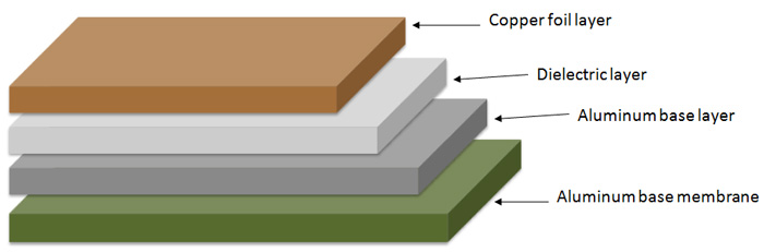
An aluminum PCB consists of a thermally conductive aluminum core, a thin dielectric layer, and a copper circuit layer bonded together. The aluminum base efficiently transfers heat away from components, preventing hotspots that could lead to failures in high-current circuits. Unlike traditional FR4 boards, aluminum PCBs excel in environments with elevated operating temperatures, making them essential for power supplies, inverters, and motor drives. For electric engineers, selecting aluminum PCBs reduces the need for bulky heatsinks and improves overall system efficiency. Factory-driven insights reveal that proper fabrication aligns with performance specs, ensuring the board meets thermal cycling demands in real-world deployments.
Material Preparation and Lamination in Aluminum PCB Fabrication
The aluminum PCB fabrication begins with selecting high-purity aluminum substrates, typically 1 to 2 mm thick, paired with a ceramic-filled epoxy dielectric and copper foil of 1 to 3 oz weight. The aluminum surface undergoes cleaning to remove oxides, followed by roughening for better adhesion. The dielectric prepreg is then placed between the aluminum and copper foil, and the stack undergoes high-pressure lamination at controlled temperatures to form a solid laminate. This bonding process creates a robust thermal pathway from traces to the base. Engineers must consider the dielectric's thermal conductivity, often above 1 W/mK, to match application needs. Quality checks at this stage verify bond strength and uniformity.
Aluminum PCB Drilling: Precision Hole Formation
Aluminum PCB drilling follows lamination and requires specialized carbide or diamond-coated tools to penetrate the copper, dielectric, and aluminum layers cleanly. Holes serve as vias for electrical connections or mounting points, but drilling through the metal core risks burrs and misalignment. Controlled feed rates and peck drilling cycles minimize heat buildup and delamination. For through-holes reaching the aluminum, subsequent desmearing removes resin residue using plasma or chemical methods. Deburring ensures smooth edges, preventing shorts during assembly. This step demands tight tolerances to comply with IPC-A-600 acceptability criteria for hole quality and registration.
Plating and Circuit Imaging Before Etching
After drilling, electroless copper plating deposits a thin conductive layer on hole walls to enable via conductivity, especially for designs bridging to the aluminum base. A dry film photoresist coats the panel, and artwork films expose the resist under UV light, hardening areas where copper remains. Development removes unexposed resist, revealing the circuit pattern. This preparation sets the stage for etching and requires precise alignment to avoid opens or shorts. Engineers appreciate how imaging resolution affects trace integrity in dense layouts.
Aluminum PCB Etching Process: Defining the Circuits
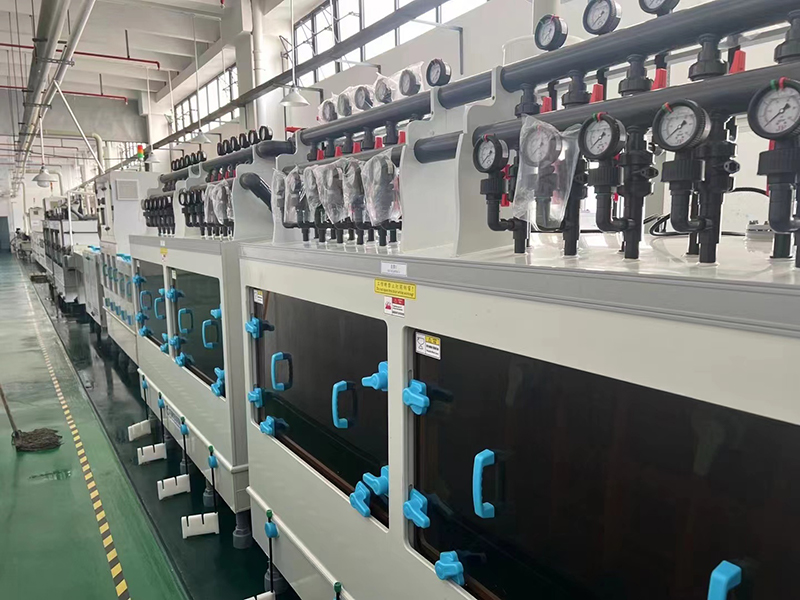
The aluminum PCB etching process selectively removes unwanted copper using alkaline or acid-based solutions, typically ferric chloride or cupric chloride, in a spray or immersion system. Etch rates are controlled to undercut minimally, preserving fine features down to 0.15 mm lines. Post-etch, the panel strips remaining photoresist via chemical solvents, followed by a micro-etch to clean traces. Differential etching accounts for copper thickness variations across the panel. Rinse and dry steps prevent corrosion. This phase demands conveyor speed adjustments for uniform results, directly impacting yield.
Aluminum PCB Solder Mask Application: Protection and Insulation
Aluminum PCB solder mask application uses liquid photoimageable (LPI) or dry film to coat the etched board, defining solder pads and protecting traces from oxidation and bridging. The mask cures via UV exposure and development, with multiple prints ensuring coverage over high-current paths. Thermal cure hardens the mask for durability. White or black masks enhance contrast for LED applications. Mask registration verifies alignment with pads per IPC-6012 performance specifications. Engineers value solder mask's role in preventing solder wicking into vias during reflow.
Final Processing: Silkscreen, Surface Finish, and Routing
Silkscreen printing adds component legends using epoxy ink, baked for adhesion. Surface finishes like HASL, ENIG, or OSP protect exposed copper from tarnish while aiding solderability. Routing or V-scoring outlines individual boards from panels, with tabs for fixturing. Electrical testing probes nets for continuity and shorts. Visual and automated optical inspections confirm quality. These steps finalize the bare board ready for population.
Aluminum PCB Assembly: Integrating Components
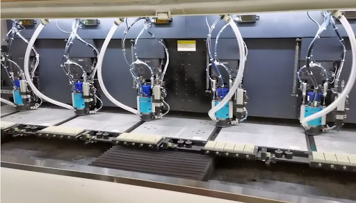
Aluminum PCB assembly starts with stencil printing of solder paste on pads, followed by pick-and-place of SMD components. Reflow soldering melts paste, but the aluminum core accelerates cooling, requiring profile adjustments to avoid warpage. Through-hole parts insert next, secured by wave soldering or selective methods. The metal base acts as a natural heatsink, distributing heat evenly. Post-assembly cleaning removes flux residues. Inspection per J-STD-001 ensures joint integrity, especially for power devices. Factory experience shows thermal vias enhance dissipation during assembly.
Best Practices for Aluminum PCB Fabrication and Design
Engineers should incorporate thermal vias under hot components to channel heat to the aluminum core effectively. Avoid blind vias unless specified, as they complicate drilling. Specify panelization with breakaway tabs for handling. Select dielectric with matching CTE to aluminum to minimize stress. Prototype runs validate etch factors and mask adhesion. Collaborate with fabricators early on stackup details. These practices boost reliability in demanding electric applications.
Conclusion
The aluminum PCB manufacturing process, from lamination through aluminum PCB assembly, balances thermal excellence with electrical precision. Key steps like aluminum PCB drilling, etching, and solder mask ensure boards withstand operational stresses. Electric engineers benefit from factory-aligned designs that leverage standards for consistent outcomes. Mastering these insights enables smarter choices in high-power projects, enhancing performance and longevity.
FAQs
Q1: What is the aluminum PCB etching process, and why is it critical?
A1: The aluminum PCB etching process removes excess copper after imaging to form traces, using controlled chemical solutions for clean profiles. It is critical because poor etching leads to overcuts or residues, compromising conductivity and reliability. Factories optimize conveyor speeds and chemistry for uniform results across panels. Engineers design with etch compensation to achieve fine pitches reliably.
Q2: How does aluminum PCB drilling differ from standard PCBs?
A2: Aluminum PCB drilling penetrates metal cores, requiring robust tools and peck cycles to avoid burrs or delamination. Unlike FR4, it risks heat-induced warping, so coolant and parameters are adjusted. Desmearing follows to clear dielectric debris. This ensures via quality for interconnections. Proper execution meets hole wall roughness specs.
Q3: What role does aluminum PCB solder mask play in fabrication?
A3: Aluminum PCB solder mask insulates traces, defines pads, and protects against environmental factors during assembly. Applied post-etching, it cures to withstand reflow temperatures. It prevents solder bridging in dense layouts. White variants aid optical inspection in lighting applications. Alignment precision safeguards pad exposure.
Q4: What considerations apply to aluminum PCB assembly?
A4: Aluminum PCB assembly demands reflow profiles accounting for rapid base cooling to prevent defects like head-in-pillow. Thermal pads interface components to the core effectively. J-STD-001 guides joint quality checks. Avoid excessive flux to minimize cleaning needs. These ensure robust power handling.
References
IPC-A-600K — Acceptability of Printed Boards. IPC, 2020
IPC-6012E — Qualification and Performance Specification for Rigid Printed Boards. IPC, 2015
J-STD-001H — Requirements for Soldered Electrical and Electronic Assemblies. IPC/JEDEC, 2018


