What Role Does a PCB Stackup Play in Board Design?
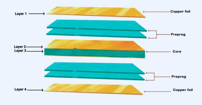
A Printed Circuit Board (PCB) stackup defines the precise arrangement of conductive copper layers and insulating dielectric materials, such as prepreg and core, within a multi-layer board. These layers are meticulously organized to serve distinct functions: signal layers carry electrical traces, power planes distribute voltage, and ground planes offer shielding and reduce noise. The specific configuration of these layers, whether balanced or unbalanced, profoundly influences the board's operational characteristics, ease of manufacturing, and overall cost.
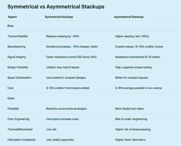
The architecture of a stackup directly affects crucial performance metrics like signal integrity, electromagnetic compatibility (EMC), heat dissipation, and structural stability. An intelligently designed stackup can effectively mitigate common problems such as crosstalk, impedance mismatches, and board warping. Conversely, a poorly planned stackup can lead to expensive redesigns or even product failures. Understanding the fundamental distinctions between symmetrical and asymmetrical stackups is the initial step toward optimizing your PCB for both performance and budgetary considerations.
What Are the Key Differences Between Symmetrical and Asymmetrical Stackups?
Before delving into the specific benefits and drawbacks of each approach, it's essential to clearly define symmetrical and asymmetrical stackups and highlight their core distinctions.
Understanding Symmetrical Stackups
A symmetrical stackup is characterized by an even and balanced distribution of layers above and below the central axis of the quick turn PCB. For instance, in an eight-layer board, there might be four conductive and dielectric layers on the top half that mirror the four layers on the bottom half. This balanced arrangement ensures uniform thickness and consistent material properties throughout the board's cross-section.
Understanding Asymmetrical Stackups
Conversely, an asymmetrical stackup lacks this intrinsic balance. The layers are not evenly distributed, meaning one side of the board might contain a different quantity or type of copper or dielectric material than the other. For example, a 6 layer board could have four layers configured on one side and two on the opposite side, resulting in an uneven structural composition.
Core Distinctions at a Glance
● Layer Distribution: Symmetrical designs feature balanced layers; asymmetrical ones do not.
● Thermal Behavior: Symmetrical boards expand uniformly when exposed to heat, whereas asymmetrical designs may warp due to uneven internal stresses.
● Manufacturing Ease: Symmetrical stackups are generally simpler and more cost-effective to produce, while asymmetrical configurations often demand specialized processes.
● Application Suitability: Symmetrical stackups are suitable for most standard applications, while asymmetrical ones cater to specific requirements like unique trace routing or spatial limitations.
What Are the Benefits and Drawbacks of Asymmetrical Stackups?
Exploring the advantages and disadvantages of asymmetrical stackups is crucial for designers considering this less conventional approach for their PCB projects.
Advantages of Asymmetrical Stackups
● Enhanced Design Flexibility: Asymmetrical configurations allow engineers to strategically place critical layers, such as high-speed signal layers, closer to one surface of the board. This enables accommodation of unique routing demands or optimized component placement.
● Optimized Space Utilization: In devices with severe space constraints, an asymmetrical stackup can help integrate more functionality into a limited area by tailoring layer distribution to specific layout requirements.
● Potential Cost Reductions: In certain scenarios, reducing the number of layers or specific materials on one side of the board might lead to lower material costs. However, actual savings depend heavily on manufacturing capabilities and production volumes. For example, a design requiring fewer overall layers on one side could reduce copper and dielectric expenses by 5-10% in smaller production runs.
Disadvantages of Asymmetrical Stackups
● Thermal and Mechanical Stability Issues: The uneven distribution of layers can cause differential thermal expansion, leading to board warping during critical processes like soldering or during operational use. The risk of warping can increase by up to 20% in asymmetrical designs when subjected to high temperatures, such as during reflow soldering at 260°C.
● Increased Manufacturing Complexity: Many PCB fabrication houses prioritize symmetrical designs due to their standardized processes. Asymmetrical stackups often necessitate custom setups, potentially extending lead times and increasing manufacturing costs by 10-15% for smaller batches.
● Challenges in Signal Integrity: Uneven layer structures can complicate impedance control, especially for high-speed signals exceeding 1 GHz. This can lead to impedance mismatches of 5-10 ohms if not meticulously managed, impacting signal quality.
What Are the Benefits and Drawbacks of Symmetrical Stackups?
To offer a comprehensive comparison, let's also examine the strengths and weaknesses associated with symmetrical PCB stackups, highlighting why they remain a popular choice.
Advantages of Symmetrical Stackups
● Superior Thermal Stability: The balanced arrangement of layers ensures consistent expansion and contraction under thermal stress. This significantly minimizes the risk of board warping, potentially reducing it by up to 30% compared to asymmetrical designs.
● Simplified Manufacturing Processes: Symmetrical designs integrate seamlessly with standard fabrication procedures, often resulting in lower production costs (up to 10% savings) and quicker turnaround times.
● Optimized Signal Integrity: The uniform structure of symmetrical stackups simplifies impedance matching and effectively reduces crosstalk between traces. This makes them highly suitable for high-speed designs that demand strict tolerances, such as maintaining a controlled impedance of 50 ohms with a ±5% deviation.
Disadvantages of Symmetrical Stackups
● Limited Design Adaptability: Symmetrical constraints might necessitate design compromises in trace routing or component placement, particularly for projects with unconventional layout requirements.
● Risk of Over-Engineering: Occasionally, designers might add unnecessary layers simply to maintain symmetry, which can inflate costs. This "over-engineering" can sometimes increase material expenses by 8-12% for smaller production batches.
How to Choose the Right PCB Stackup for Your Design
Selecting the optimal stackup, whether symmetrical or asymmetrical, demands a careful evaluation of your project's specific objectives and constraints. Adhering to certain best practices can guide this crucial decision-making process.
Key Considerations for Stackup Selection
● Evaluate Application Requirements: Begin by thoroughly assessing the electrical, mechanical, and thermal demands of your PCB application. For high-speed designs (e.g., data transfer rates above 5 Gbps), a symmetrical stackup often proves superior due to its inherent consistency in impedance control. Conversely, for designs with tight space limitations or highly customized layouts, an asymmetrical approach might offer the necessary flexibility.
● Prioritize Signal Integrity: For modern electronics processing high-frequency signals, signal integrity is paramount. Leverage simulation tools to accurately model impedance and potential crosstalk. For example, achieving a stable differential pair impedance of 100 ohms for USB 3.0 interfaces is typically more straightforward with a symmetrical stackup due to uniform layer spacing.
● Account for Thermal Management: If the PCB will operate in demanding thermal environments or undergo multiple reflow soldering cycles, symmetrical stackups are preferred as they significantly reduce the likelihood of warping. Empirical studies indicate that asymmetrical designs can exhibit bowing up to 0.5 mm in a 100 mm x 100 mm board under thermal stress, compared to only 0.2 mm for symmetrical counterparts.
● Engage with Your Manufacturer Early: Proactive communication with your PCB fabrication partner is indispensable. Be aware that some manufacturers might levy higher charges for asymmetrical stackups due to the need for specialized processing steps. Discuss various stackup options to ensure your design aligns with their manufacturing capabilities, thereby avoiding unforeseen costs or delays.
What Are the Cost Implications of Symmetrical vs. Asymmetrical Stackups?
Cost remains a pivotal factor in any PCB development project. A detailed cost analysis for both stackup types can help in effective budget planning.
Breaking Down the Cost Factors
● Material Expenses: Symmetrical stackups often benefit from using more standardized materials across all layers, which can simplify procurement and potentially lower overall material costs. While asymmetrical designs might reduce material consumption by having fewer layers on one side, this saving can be negated by the need for custom dielectric thicknesses. On average, material costs for asymmetrical stackups could be 5-8% higher due to their non-standard configurations.
● Manufacturing Costs: Fabrication expenses are typically lower for symmetrical stackups because they conform to standard production processes. For instance, a six-layer symmetrical board might cost approximately $50 per square foot for small production volumes, whereas an asymmetrical design could increase to
● 60 due per square foot due to the additional setup time and specialized procedures. In large-scale production, these price differences may narrow but still contribute to the total expenditure.Yield and Reliability: Asymmetrical stackups can sometimes result in lower manufacturing yields due to issues like warping or delamination, potentially escalating costs by 3-5% from increased rework or scrap rates. Symmetrical stackups, known for their higher inherent reliability, mitigate these risks, leading to long-term cost savings.
When is an Asymmetrical Stackup the Right Choice for Your PCB?
While symmetrical stackups are often the go-to default for most PCB projects, specific design scenarios can strongly favor an asymmetrical approach.
Ideal Scenarios for Asymmetrical Stackups
● Specialized Routing Demands: If your design necessitates certain layers to be positioned closer to one surface of the board—for example, to optimize performance for high-frequency RF components operating at 2.4 GHz—an asymmetrical stackup can effectively accommodate these precise requirements.
● Ultra-Compact Designs: In the development of exceptionally small devices, such as wearable technology, asymmetrical stackups offer a strategic advantage by enabling the integration of complex circuitry within extremely limited spatial envelopes.
● Cost-Focused Prototyping: For initial prototypes where the primary objective is to minimize upfront expenses, even if it entails a slight compromise on long-term reliability, an asymmetrical design might offer a more economical starting point.
However, it is crucial to carefully weigh these potential benefits against inherent risks like thermal instability and increased manufacturing challenges. When uncertainty exists, a symmetrical stackup generally remains the safer and more reliable choice.
Final Considerations on PCB Stackup Selection
The decision between an asymmetrical and symmetrical stackup is a pivotal one, directly influencing your PCB's performance, overall reliability, and production cost. While asymmetrical stackups provide a degree of flexibility for highly specialized designs, they come with inherent trade-offs regarding thermal stability and manufacturing complexity. In contrast, symmetrical stackups offer a balanced approach, simplifying production and making them suitable for the majority of applications.
By diligently applying PCB design best practices—such as thoroughly evaluating your application's specific needs, prioritizing signal integrity, and fostering early collaboration with your manufacturing partner—you can arrive at an informed and strategic decision. Furthermore, a comprehensive PCB cost analysis ensures that your chosen stackup aligns perfectly with your project's budgetary constraints. Whether your final choice leans towards an asymmetrical or symmetrical configuration, the ultimate goal is to tailor your design precisely to the unique demands of your project.
AIVON is dedicated to supporting your PCB design journey, offering expert guidance and superior manufacturing solutions. We invite you to explore the nuances of symmetrical versus asymmetrical stackup options, and allow us to assist you in realizing your vision with unparalleled precision and efficiency.


