Introduction
High-frequency printed circuit boards (PCBs) form the backbone of modern applications in telecommunications, radar systems, and high-speed data processing. These boards operate at frequencies often exceeding several gigahertz, where signal integrity becomes paramount to prevent data errors and system failures. PCB testing techniques such as time-domain reflectometry (TDR) and vector network analyzer (VNA) measurements ensure that traces maintain controlled impedance and minimal losses. Without rigorous testing, issues like reflections, crosstalk, and attenuation can degrade performance, leading to unreliable signal transmission. Engineers rely on these methods to validate designs against specifications, bridging the gap between simulation and real-world operation. This article explores essential testing approaches, focusing on signal integrity, impedance control, and S-parameters for optimal high-frequency PCB performance.
Why Signal Integrity Testing Matters for High-Frequency PCBs
Signal integrity refers to the preservation of electrical signal quality across a PCB transmission line. At high frequencies, phenomena such as skin effect, dielectric losses, and impedance mismatches amplify distortions, causing reflections that corrupt data. For instance, when signal rise times approach or fall below one-tenth of the trace length's propagation delay, even minor discontinuities can lead to significant bit error rates. PCB testing identifies these vulnerabilities early, ensuring compliance with performance requirements. Impedance control is critical, as mismatches result in return loss that attenuates signals and generates electromagnetic interference. Ultimately, thorough signal integrity validation supports higher data rates and reliable operation in demanding environments.
High-frequency PCBs demand precise characterization because material properties vary with frequency. Dielectric constant and loss tangent shift, impacting propagation velocity and attenuation. Without proper testing, engineers risk overlooking issues like via stubs or plane resonances that degrade S-parameters. Industry practices emphasize test coupons integrated into panel designs for representative measurements. These techniques not only verify manufacturing quality but also guide design iterations for improved yield.
Fundamentals of Impedance Testing in High-Frequency PCBs
Impedance in PCB traces is the characteristic value that determines how signals propagate without reflection. For high-frequency applications, single-ended traces typically target 50 ohms, while differential pairs aim for 100 ohms. Variations arise from trace width, thickness, dielectric height, and material properties. Accurate measurement prevents signal bounce, which manifests as overshoot or ringing in waveforms. Engineers use controlled test structures to isolate these parameters during validation. Consistent impedance ensures predictable behavior across frequencies.
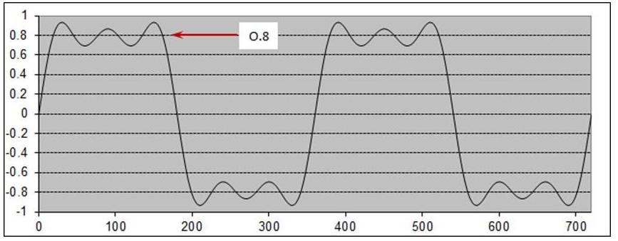
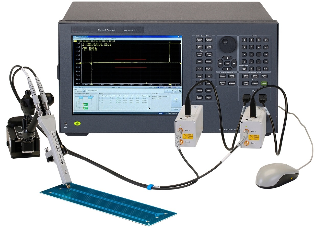
Time-domain reflectometry (TDR) serves as a primary tool for impedance profiling. It launches a fast-rising step signal into the trace and analyzes reflections caused by discontinuities. Positive reflections indicate higher impedance, while negative ones signal lower values. Rise times below 35 picoseconds enable resolution of fine features like vias. TDR provides spatial information, pinpointing exact locations of mismatches along the line. This method excels in production environments for quick pass-fail decisions.
Time-Domain Reflectometry (TDR): Principles and Applications
TDR operates on the principle of radar-like echo analysis in transmission lines. A pulse generator sends an incident wave, and any impedance change causes partial reflection according to the reflection coefficient formula, Gamma equals (Z_load minus Z0) over (Z_load plus Z0). The time delay of the reflection reveals the distance to the fault, calculated via velocity factor. For PCBs, velocity factors range from 0.6 to 0.7 times the speed of light, depending on the laminate. Calibration with open, short, and load standards establishes the reference plane. This setup aligns measurements to the device under test, minimizing fixture effects.
In practice, TDR testing follows standardized procedures to ensure repeatability. Test coupons with microstrip or stripline geometries mimic production traces. Launch conditions, such as solderless probes or SMA connectors, preserve signal fidelity. Bandwidth limitations from sampling oscilloscopes must match the application's frequency content. Interpretation involves correlating waveform steps to design values, flagging deviations beyond tolerance. TDR complements simulations by validating extracted models for further analysis.
High-frequency TDR requires attention to bandwidth and de-embedding. Extraneous reflections from connectors demand subtraction via mathematical models. Differential TDR extends this to pairs, revealing mode conversion issues. Effective length calculations guide coupon design, ensuring coverage of critical nets. Regular calibration maintains accuracy across batches. These steps uphold quality in volume production.
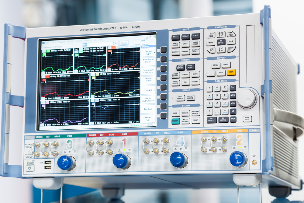
S-Parameters and Vector Network Analyzer (VNA) Measurements
S-parameters describe linear network behavior in the frequency domain, essential for high-frequency PCB testing. S11 represents return loss, quantifying reflected power, while S21 measures insertion loss or transmission. Crosstalk appears in S31 or S41 for near- and far-end coupling. These parameters capture magnitude and phase, enabling full characterization up to 40 GHz or higher. VNAs sweep sinusoidal signals across frequencies, comparing incident and reflected waves via directional couplers. Vector error correction through calibration yields precise results.
VNA advantages over pure time-domain tools include superior dynamic range and phase accuracy. Narrow intermediate frequency bandwidths suppress noise, revealing subtle crosstalk below -60 dB. Time-domain transforms via inverse Fourier allow TDR-like views from frequency data. Band-limited step or impulse responses simulate real signals. Multiport configurations handle complex interconnects with 16 or more S-parameters. This versatility supports backplane and package analysis.
Calibration techniques like SOLT (short, open, load, thru) establish reference planes at connectors. TRL (thru-reflect-line) suits on-board fixtures with unknown lines. De-embedding removes fixture parasitics, isolating true PCB response. Automated software streamlines data processing, generating eye diagrams from S-parameters. Compliance masks verify against limits for insertion loss or return loss. These practices ensure signal integrity across the full bandwidth.
IPC-TM-650 outlines methods for such VNA-based high-frequency evaluations, providing guidelines for attenuation and phase measurements up to 10 GHz.
Best Practices for High-Frequency PCB Testing
Integrate test coupons strategically on panels to represent diverse trace geometries. Microstrip for surface signals, stripline for embedded routes. Lengths should exceed three times the rise time distance for clean TDR. Ground planes beneath prevent radiation. Fabrication tolerances demand verification post-plating. Pre-defined via fences minimize resonances.
Calibration remains foundational for all measurements. Perform full two-port calibrations before each session. Verify with known standards periodically. Fixture design incorporates low-loss launches and repeatable connections. Automated test equipment accelerates throughput in factories. Data logging supports statistical process control.
Combine TDR and VNA for comprehensive insights. TDR localizes issues, VNA quantifies frequency dependence. Post-process S-parameters into time-domain for correlation. Tolerance bands account for material variations. IPC-6012E specifications guide acceptance criteria for rigid board performance, including high-frequency attributes.
Environmental conditioning precedes testing to simulate service life. Thermal cycling reveals CTE mismatches affecting impedance. Humidity tests expose absorption effects on dielectrics. Correlate with baseline dry measurements. Iterative feedback refines processes.
Troubleshooting Signal Integrity Issues
Common TDR anomalies include via stubs showing step-down reflections. Extend or back-drill to mitigate. Plane splits cause periodic ripples, resolved by stitching vias. Crosstalk peaks in VNA far-end S41 demand guard traces or shielding. Insertion loss roll-off signals dielectric losses, prompting low-Dk materials.
Lossy traces exhibit gradual TDR droop. Frequency sweeps confirm conductor skin effect dominance. Modeled de-embedding isolates contributions. Jitter budgets incorporate these margins. Systematic root cause analysis traces to stackup or plating variations.
Conclusion
Mastering PCB testing techniques like TDR and VNA ensures high-frequency boards deliver robust signal integrity. Impedance control, S-parameter analysis, and time-domain reflectometry pinpoint and resolve issues efficiently. Adhering to best practices, including precise calibration and test structures, aligns production with design intent. These methods safeguard performance in gigahertz regimes, reducing field failures. Engineers gain confidence through data-driven validation, enabling innovation in high-speed electronics.
FAQs
Q1: What is time-domain reflectometry (TDR) in PCB testing?
A1: TDR sends a step pulse along PCB traces to detect impedance discontinuities via reflections. The reflection coefficient reveals mismatch locations by time delay, aiding signal integrity verification. Calibration sets the reference, while velocity factor computes distances accurately. This technique excels for high-frequency impedance control without full assembly.
Q2: How do S-parameters contribute to high-frequency PCB testing?
A2: S-parameters characterize reflection (S11) and transmission (S21) across frequencies using a VNA. They quantify losses, crosstalk, and phase shifts critical for signal integrity. Multiport measurements handle differential pairs effectively. De-embedding isolates board response from fixtures. Compliance checks ensure design margins.
Q3: What role does a vector network analyzer (VNA) play in impedance testing?
A3: VNAs measure S-parameters precisely, transforming to time-domain for TDR-like impedance profiles. Superior dynamic range detects subtle issues like low-level crosstalk. Calibration methods like SOLT enhance accuracy up to millimeter waves. They support full channel analysis for high-speed PCBs.
Q4: Why is signal integrity crucial in high-frequency PCB testing?
A4: Signal integrity prevents reflections and losses that degrade data rates in gigahertz applications. Testing via TDR and VNA identifies impedance mismatches early. It ensures reliable transmission amid skin effect and dielectric variations. Factory validation boosts yield and performance.
References
IPC-TM-650 - Test Methods Manual. IPC.
IPC-6012E - Qualification and Performance Specification for Rigid Printed Boards. IPC, 2017.
IPC-6018D - Qualification and Performance Specification for High Frequency (Microwave) Printed Boards. IPC, 2020.


