Introduction
Microvia placement stands as a critical skill in modern printed circuit board design, especially for electronic hobbyists aiming to create compact, high performance circuits. As devices shrink and component density rises, microvias offer a way to connect layers in a PCB with precision, enabling complex designs in limited space. This article explores the essence of microvia placement, often considered an art due to the balance of technical rules and creative problem solving it demands. Hobbyists can benefit from understanding these tiny vias, which facilitate high density interconnects while maintaining signal integrity. We'll cover the principles behind microvias, best practices for placement, and practical tips tailored for enthusiasts working on personal projects. Whether you're designing a small gadget or experimenting with advanced layouts, mastering this technique elevates your PCB craftsmanship.
What Are Microvias and Why Do They Matter
Microvias are small diameter vias, typically less than 0.15 millimeters, used to connect different layers in a multilayer PCB. Unlike traditional through hole vias that span the entire board thickness, microvias connect only adjacent layers or a few layers, minimizing space usage. They are essential in high density interconnect technology, allowing designers to pack more functionality into smaller footprints. For electronic hobbyists, this means the ability to design sophisticated circuits for compact devices like wearables or IoT gadgets.
The importance of microvias lies in their impact on signal integrity and board reliability. Properly placed microvias reduce signal path length, cutting down on interference and improving performance in high speed applications. They also help manage thermal dissipation by providing efficient pathways. For hobbyists, using microvias can be a game changer, turning a bulky prototype into a sleek, professional grade design. Understanding their role is the first step toward leveraging their benefits in personal projects.
Related Reading: Microvia Design for EMI Reduction
Technical Principles of Microvia Placement
Microvia placement involves understanding both electrical and mechanical constraints in PCB design. At the core, microvias must ensure reliable interlayer connections without compromising the board's structural integrity. They are often created using laser drilling, which allows precise control over size and depth, unlike mechanical drilling used for larger vias. This precision is crucial for maintaining alignment between layers, especially in dense layouts common in hobbyist projects with limited space.
Electrically, microvias affect signal transmission. Their small size reduces parasitic capacitance and inductance, beneficial for high frequency signals. However, incorrect placement can lead to signal reflection or crosstalk if they are too close to sensitive traces. Mechanically, microvias must be positioned to avoid stress points that could cause cracking during thermal cycles or board flexing. Standards like IPC-2226, which focuses on high density interconnect design, provide guidelines for aspect ratios and spacing to ensure reliability.
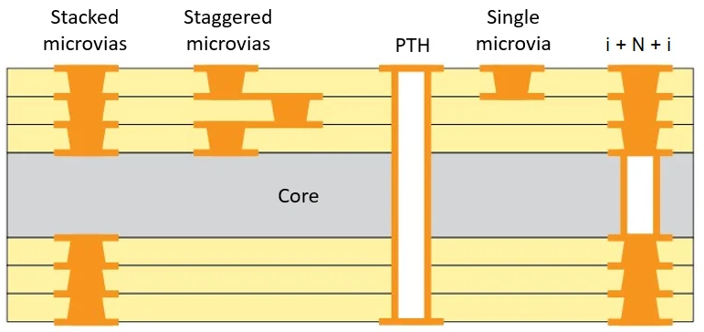
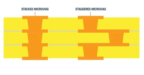
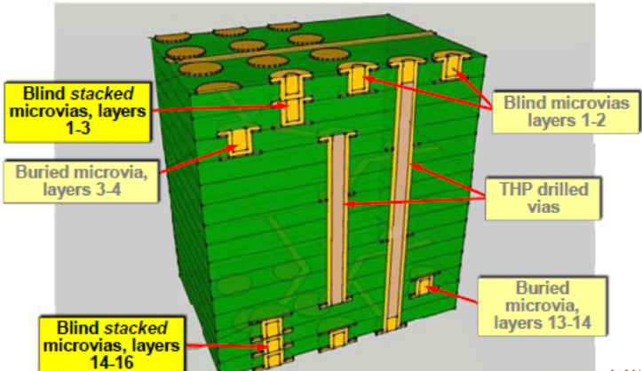
Hobbyists must also consider the stackup configuration. Stacked microvias, where multiple microvias are aligned vertically across layers, can save space but may pose reliability risks if not designed per industry standards. Staggered microvias, placed offset from each other, often offer better structural stability. Balancing these factors requires careful planning during the design phase to avoid issues in fabrication or operation.
Related Reading: Microvia PCB Design Rules: A Practical Handbook for Error Free HDI Layouts
Best Practices for Microvia Placement
For electronic hobbyists, placing microvias effectively involves adhering to practical guidelines that balance design needs with manufacturing capabilities. Start by defining the layer stackup early in the design process. Determine which layers need interconnection and plan microvia locations to minimize signal path length. This reduces latency and potential interference, crucial for high speed hobbyist projects like radio frequency circuits.
Follow aspect ratio guidelines as outlined in standards such as IPC-2226. This standard recommends keeping the ratio of microvia depth to diameter low, typically below 1:1, to ensure manufacturability and reliability. For hobbyists using affordable fabrication services, sticking to conservative ratios prevents issues like incomplete drilling or plating defects. Always check with fabrication capabilities before finalizing designs to avoid costly revisions.
Position microvias away from high stress areas, such as board edges or under heavy components. This reduces the risk of mechanical failure during assembly or use. Additionally, maintain adequate spacing between microvias and nearby traces or pads to prevent electrical shorts or interference. Use ground planes strategically near microvias to shield signals and improve electromagnetic compatibility, a tip especially useful for hobbyists working on noise sensitive designs.
Consider thermal management when placing microvias. Grouping them in areas with good heat dissipation paths helps avoid localized overheating. For multilayer boards, distribute microvias evenly to prevent warping due to uneven copper distribution. Software tools adhering to industry standards can simulate these effects, helping hobbyists visualize potential problem areas before fabrication.
Finally, always verify designs against standards like IPC-A-600K for acceptability criteria. This ensures that microvia placement meets quality benchmarks, reducing the likelihood of defects. For hobbyists, iterating designs with these practices in mind transforms microvia placement into an art, blending technical precision with creative layout solutions.
Troubleshooting Common Microvia Placement Issues
Hobbyists often encounter challenges when integrating microvias into their designs, especially without access to advanced tools or extensive experience. One common issue is misalignment during layer registration, leading to poor connections. To address this, ensure that design files specify tight tolerances for layer alignment, referencing guidelines from IPC-6012E for rigid board performance. Double check drill files to confirm microvia positions match across layers.
Another frequent problem is microvia failure under thermal stress. If a board undergoes significant temperature changes during soldering or operation, microvias may crack. Mitigate this by selecting materials with compatible thermal expansion properties and adhering to aspect ratio limits per IPC-2226. Testing prototype boards under simulated conditions can reveal potential weaknesses before full production.
Signal integrity issues also arise if microvias are placed too close to high speed traces. This can cause crosstalk or impedance mismatches. Use simulation tools to model signal behavior and adjust placement to maintain clear signal paths. Ground vias near microvias can act as shields, a practical fix for hobbyists dealing with electromagnetic interference in compact designs.
Lastly, fabrication limitations often catch hobbyists off guard. Some low cost services may not support microvias below a certain size or in complex stackups. Always review manufacturer specifications and design within those constraints. By anticipating these issues and applying standards like IPC-A-600K for inspection criteria, hobbyists can refine their approach to microvia placement, ensuring functional and reliable PCBs.
Conclusion
Mastering the art of microvia placement empowers electronic hobbyists to push the boundaries of PCB design, creating compact and efficient circuits for innovative projects. By understanding the technical principles behind microvias, adhering to best practices, and troubleshooting common issues, enthusiasts can achieve professional quality results even with limited resources. Standards such as IPC-2226 and IPC-A-600K provide a solid foundation for ensuring reliability and performance. As you experiment with denser layouts and high speed applications, thoughtful microvia placement becomes a blend of science and creativity, enhancing both functionality and aesthetics in your designs. Keep refining your skills with each project to turn challenges into opportunities for learning and improvement.
FAQs
Q1: What is the importance of microvia placement in PCB design for hobbyists?
A1: Microvia placement is crucial for hobbyists as it enables compact, high density designs in limited space. Proper placement ensures signal integrity, reduces interference, and improves thermal management. By mastering this art, hobbyists can build advanced circuits for small devices like wearables, ensuring reliable performance without bulky layouts, all while adhering to basic design principles.
Q2: How can I avoid errors in microvia placement during my projects?
A2: To avoid errors in microvia placement, plan your layer stackup early and follow aspect ratio guidelines from standards like IPC-2226. Keep microvias away from stress points and ensure spacing from traces. Check fabrication limits and use simulation tools to predict issues. Reviewing designs against acceptability criteria helps catch mistakes before production.
Q3: What standards should guide microvia placement for reliable results?
A3: Standards like IPC-2226 for high density interconnect design and IPC-A-600K for acceptability of printed boards are essential for microvia placement. They provide guidelines on aspect ratios, spacing, and quality criteria. Hobbyists can rely on these to ensure designs are manufacturable and reliable, avoiding common pitfalls in personal projects.
Q4: Why is microvia placement considered an art in PCB design?
A4: Microvia placement is seen as an art because it combines strict technical rules with creative problem solving. Hobbyists must balance electrical performance, mechanical stability, and fabrication constraints while optimizing layouts. This blend of precision and ingenuity transforms a functional necessity into a skillful design process, unique to each project's needs.
References
IPC-2226 - Design Standard for High Density Interconnect (HDI) Printed Boards. IPC, 2003.
IPC-A-600K - Acceptability of Printed Boards. IPC, 2020.
IPC-6012E - Qualification and Performance Specification for Rigid Printed Boards. IPC, 2020.


