Introduction
In modern PCB manufacturing, high-speed signal transmission demands precise control over via structures to maintain integrity. Controlled depth drilling, often referred to as backdrilling, addresses via stub issues that degrade performance in multilayer boards. This technique involves drilling from the opposite side of a through-hole via to a specific depth, removing unused copper barrel portions. While it introduces additional PCB manufacturing expenses, the potential for enhanced signal integrity justifies evaluation. This article examines the controlled depth drilling cost alongside its benefits, providing electric engineers with a balanced view for PCB design optimization. Factory insights reveal that strategic application can yield substantial backdrilling ROI in demanding applications.
What Is Controlled Depth Drilling and Why Does It Matter?
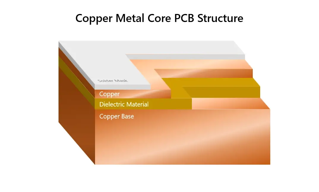
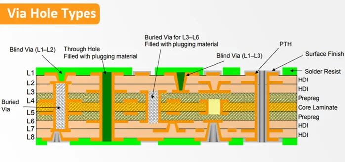
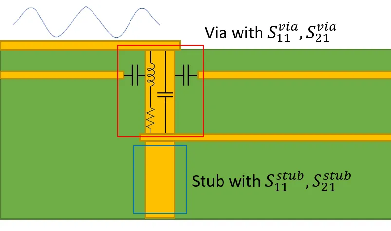
Controlled depth drilling targets the removal of via stubs, which are the extended copper lengths beyond active signal layers in plated through-holes. These stubs act as impedance discontinuities, causing signal reflections, insertion loss, and crosstalk in high-frequency designs. By precisely controlling the drill depth, manufacturers shorten the via to align with the signal path, improving return loss and eye diagram quality. This process matters increasingly as data rates exceed 10 Gbps, where conventional through-vias fail to meet signal integrity cost analysis thresholds. In production, it serves as a cost-effective alternative to blind or buried vias, especially in thick stackups. Engineers must weigh these factors during initial design to avoid costly redesigns later.
Technical Principles of Controlled Depth Drilling
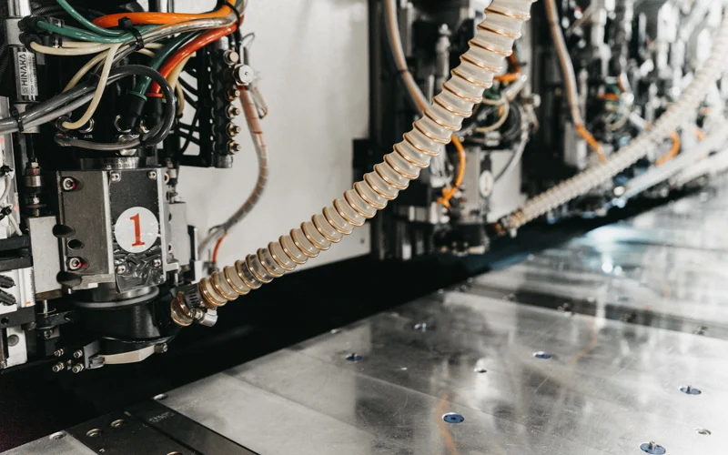
The process begins after standard through-hole drilling and plating, using a larger diameter drill bit from the non-signal side. Depth control relies on mechanical parameters like feed rate, spindle speed, and peck drilling cycles to prevent breakthrough or insufficient stub removal. Tolerances typically demand plus or minus 0.1 mm accuracy, verified through x-ray or sectioning per IPC-DR-572 drilling guidelines. The backdrill bit oversizes the original hole by 0.15 to 0.25 mm to clear plating without damaging adjacent layers. Challenges include drill wander in high-aspect-ratio boards and heat buildup, which can cause resin smear. Proper coolant use and tool geometry mitigate these, ensuring consistent results across panels.
Signal integrity improves as stub length reduces from full board thickness to under 0.5 mm, minimizing resonance effects up to 20 GHz. Factory experience shows that alignment between front and backdrill targets is critical, often guided by fiducials. Post-drilling, debris removal via plasma or chemical desmear prevents shorts. This technique integrates seamlessly into standard flows but requires dedicated tooling setups.
Factors Influencing Controlled Depth Drilling Cost
Controlled depth drilling adds layers to the production cycle, directly impacting PCB manufacturing expenses. Each backdrill operation consumes extra machine time, typically 20 to 50 percent more per panel depending on via count and board thickness. Tooling costs rise due to specialized oversized bits that wear faster under controlled depth conditions. Inspection steps, including electrical testing for opens and shorts, further escalate expenses. Yield rates can dip initially if depth control falters, leading to scrap or rework. However, batch processing multiple backdrills in one setup amortizes these costs for high-volume runs.
Material factors play a role too; thicker cores or high-Tg laminates increase drill resistance, prolonging cycles. Panel utilization drops if backdrill clearances mandate spacing around vias. Engineers optimizing designs minimize unique drill sizes to consolidate hits, reducing setup changes. Overall, controlled depth drilling cost scales with complexity, but standardization lowers per-unit impact.
Benefits and Backdrilling ROI
The primary benefit lies in superior signal integrity, where reduced stubs cut insertion loss by aligning via impedance with traces. This enables higher data rates without exotic materials or via-in-pad designs, offering clear backdrilling ROI for serdes channels. Crosstalk diminishes as stub antennas cease radiating energy, improving eye height and width in simulations. In production, it avoids the premium for HDI structures, balancing performance with manufacturability. Long-term, fewer field failures from SI issues reduce warranty costs.
Quantitative ROI emerges in applications like telecom routers or servers, where redesigns for blind vias exceed backdrilling premiums. Factory data indicates that for boards over 1.6 mm thick with 100+ high-speed vias, payback occurs within prototype iterations. Signal integrity cost analysis favors it when stub length exceeds 10 percent of wavelength. PCB design optimization incorporating backdrills early maximizes these gains.
Best Practices for Implementing Controlled Depth Drilling
Start with stackup planning to group signal layers, minimizing backdrill zones per via. Specify depth targets relative to reference layers in fab drawings, allowing 0.1 mm tolerance. Use larger backdrill diameters judiciously to preserve annular ring per IPC-6012E qualification specs. Simulate SI pre-production to confirm stub removal efficacy. In design, route critical nets away from backdrill edges to avoid pad damage.
Collaborate with fabricators on drill charts, consolidating sizes under 20 unique calls. Post-plating timing prevents copper dissolution issues. For quality, integrate automated optical inspection focused on depth uniformity. These practices curb PCB manufacturing expenses while ensuring reliability. Regular process audits align with standards, sustaining yield above 95 percent.
Cost-Benefit Tradeoffs in Real-World Scenarios
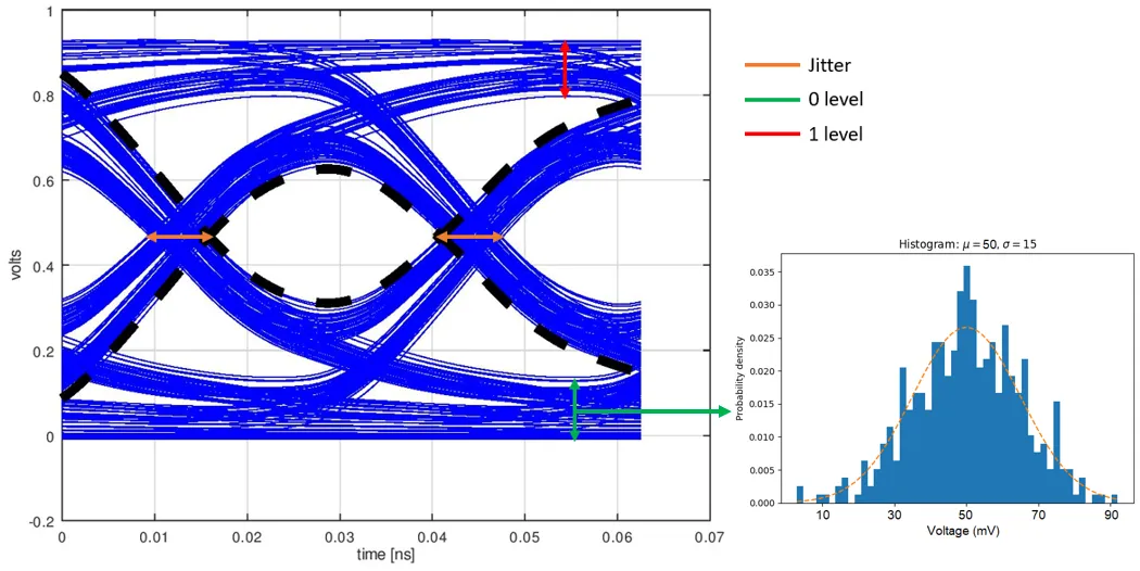
Consider a 20-layer board for 25 Gbps Ethernet; full through-vias yield -15 dB return loss, failing margins. Backdrilling inner layers improves this to -25 dB, passing at lower cost than microvias. Initial setup adds 15 percent to prototype expenses, but production scales recover via performance gains. In automotive radar modules, EMI compliance hinges on stub control, justifying the investment.
Conversely, low-speed consumer boards rarely warrant it, as costs outweigh marginal SI boosts. Engineers perform trade studies: via count times depth premium versus failure risk. Factory-driven insights emphasize panel-level optimization for ROI.
Conclusion
Controlled depth drilling presents a compelling balance in PCB production, where upfront PCB manufacturing expenses yield enduring signal integrity benefits. By shortening via stubs, it enhances high-speed performance without HDI complexity, delivering strong backdrilling ROI. Electric engineers achieve PCB design optimization through precise specifications and best practices. Factories aligned with standards like IPC-DR-572 ensure reliable execution. Ultimately, the technique proves essential for evolving demands, provided costs align with application needs.
FAQs
Q1: What factors drive controlled depth drilling cost in PCB manufacturing?
A1: Controlled depth drilling cost stems from additional machine time, specialized tooling, and enhanced inspection for depth accuracy. Oversized bits and multi-step processes increase cycle times, while yield impacts add rework potential. Design complexity, like via density, amplifies expenses, but batching mitigates per-unit rises. Optimizing drill charts reduces setups, controlling overall PCB manufacturing expenses effectively.
Q2: How does backdrilling ROI manifest in signal integrity cost analysis?
A2: Backdrilling ROI appears through reduced signal reflections and loss, enabling higher data rates without costly alternatives like blind vias. It lowers EMI risks and field failures, offsetting premiums in high-speed designs. Factory analysis shows payback in prototypes for dense via fields. Signal integrity cost analysis favors it when stubs threaten margins, optimizing long-term reliability.
Q3: What role does controlled depth drilling play in PCB design optimization?
A3: Controlled depth drilling optimizes PCB design by tailoring via lengths to signal paths, preserving impedance control in thick boards. It avoids HDI premiums while meeting high-frequency needs. Early stackup integration with fab input ensures feasibility. This approach balances performance and manufacturability seamlessly.
Q4: When should electric engineers consider controlled depth drilling?
A4: Electric engineers should opt for controlled depth drilling in multilayer boards over 1.6 mm thick with high-speed nets exceeding 10 Gbps. It is ideal when through-via stubs exceed 0.5 mm, per simulation results. Avoid in low-density or cost-sensitive low-speed applications. Consult standards for tolerances to guide decisions.
References
IPC-DR-572A — Drilling Guidelines for Printed Boards. IPC, 2007.
IPC-6012E — Qualification and Performance Specification for Rigid Printed Boards. IPC, 2015.
IPC-2221B — Generic Standard on Printed Board Design. IPC, 2003.