Introduction
In the realm of modern electronics, High Density Interconnect (HDI) PCBs have become a cornerstone for achieving compact, high performance designs. These boards enable the integration of complex circuits in smaller footprints, catering to the demands of smartphones, medical devices, and advanced computing systems. A critical element in HDI PCB design is the use of blind vias, which facilitate efficient interlayer connections without compromising space or signal integrity. For electrical engineers, understanding the role of PCB blind vias in HDI PCBs is vital to optimizing designs for both functionality and manufacturability. This article explores the significance of blind vias, their technical principles, and best practices in PCB design, providing actionable insights for professionals aiming to leverage HDI technology effectively.
What Are Blind Vias and Why Do They Matter in HDI PCBs?
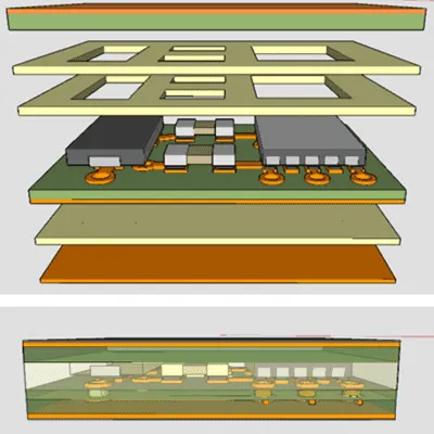
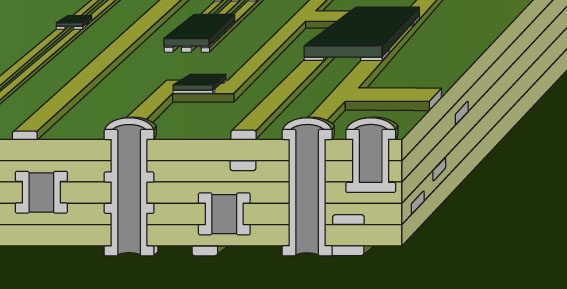
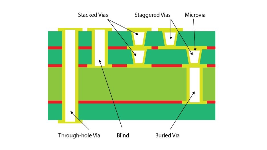
Blind vias are specialized vertical interconnects in a PCB that connect an outer layer to one or more inner layers without extending through the entire board thickness. Unlike traditional through hole vias that span all layers, PCB blind vias terminate at a specific internal layer, making them invisible from the opposite side of the board. This unique characteristic is essential for HDI PCBs, where space optimization and high component density are paramount.
The importance of blind vias lies in their ability to reduce signal path lengths and minimize interference in high speed designs. By limiting the via depth, they decrease parasitic capacitance and inductance, which are critical factors in maintaining signal integrity for high frequency applications. Additionally, blind vias allow designers to place components on both sides of the board without interference from via stubs, a common issue with through hole vias. For electrical engineers working on compact devices, integrating blind vias into PCB design ensures better routing density and improved electrical performance, aligning with the stringent requirements of modern electronics as outlined in standards like IPC-6012E.
Technical Principles of Blind Vias in HDI PCBs
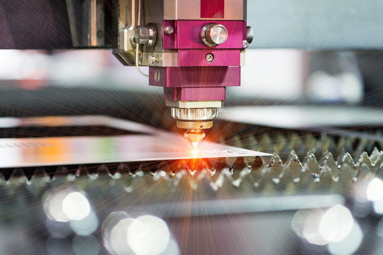
The functionality of blind vias in HDI PCBs is rooted in their construction and placement within multilayer boards. Typically, these vias are created using laser drilling technology, which allows for precise control over depth and diameter. This precision is crucial, as blind vias often have smaller aspect ratios compared to through hole vias, ensuring they meet the dimensional tolerances specified in IPC-A-600K for acceptability of printed boards.
From an electrical perspective, blind vias reduce the stub length, which is the unused portion of a via that can act as an antenna, causing signal reflections. In high speed circuits, minimizing stub effects is vital for maintaining impedance continuity. Blind vias achieve this by connecting only to the necessary layers, thus shortening the signal path. This principle is particularly beneficial in HDI PCBs, where multiple layers are stacked to accommodate dense routing.
Moreover, the use of blind vias supports sequential lamination processes in manufacturing, where layers are built up incrementally. This method, often guided by standards such as IPC-6012E, allows for the integration of microvias and blind vias at different stages, enhancing design flexibility. For electrical engineers, understanding these principles ensures that PCB design decisions align with both performance goals and manufacturing capabilities.
Related Reading: Unlocking PCB Density: A Beginner's Guide to Blind Vias
Benefits of Blind Vias in HDI PCB Design
Incorporating blind vias into HDI PCBs offers several advantages that directly impact design efficiency and product reliability. First, they enable higher component density by freeing up space on outer layers. Since blind vias do not penetrate the entire board, designers can utilize the opposite side for additional components or routing, a critical factor in miniaturized devices.
Second, blind vias improve signal integrity in high speed applications. By reducing via stubs, they minimize signal distortion and crosstalk, which are common challenges in dense layouts. This benefit is especially relevant for applications involving data rates above several gigabits per second, where maintaining signal quality is non negotiable.
Third, blind vias contribute to thermal management. In HDI PCBs, where heat dissipation is often a concern due to compact designs, blind vias can be strategically placed to connect to thermal planes without occupying excessive surface area. This approach aligns with best practices for thermal design as per industry guidelines.
Finally, blind vias support the trend toward thinner boards. By eliminating the need for through hole vias in certain areas, they allow for reduced board thickness without sacrificing connectivity. For electrical engineers, leveraging these benefits in PCB design translates to more robust and efficient electronic systems.
Challenges and Considerations in Using Blind Vias
While blind vias offer significant advantages in HDI PCBs, they also present unique challenges that electrical engineers must address during PCB design. One primary concern is the manufacturing complexity. Creating blind vias requires advanced techniques like laser drilling and precise lamination, which can increase production costs if not planned correctly. Adhering to standards such as IPC-6012E helps ensure that manufacturing processes meet quality and performance specifications.
Another challenge is the aspect ratio of blind vias. Due to their smaller size and depth, maintaining a balanced aspect ratio is critical to avoid issues like incomplete plating or structural weakness. Guidelines from IPC-A-600K provide criteria for acceptable via formation, which engineers should consult during design validation.
Reliability under thermal and mechanical stress is also a consideration. Blind vias, if not designed with proper materials and tolerances, may be susceptible to cracking or delamination during temperature cycling or board flexure. Following industry standards for material selection and testing can mitigate these risks.
Lastly, design software must accurately model blind vias to prevent errors in routing or layer alignment. Electrical engineers should ensure that design tools comply with the latest standards and support HDI specific features to avoid costly revisions. Addressing these challenges proactively ensures that blind vias enhance rather than hinder the performance of HDI PCBs.
Best Practices for Implementing Blind Vias in PCB Design
To maximize the benefits of PCB blind vias in HDI PCBs, electrical engineers should follow established best practices during the design phase. These guidelines ensure optimal performance and manufacturability while adhering to industry standards.
- Start with a clear layer stackup plan. Define which layers will use blind vias and ensure alignment with the sequential lamination process. Reference IPC-6012E for performance specifications related to multilayer construction.
- Optimize via placement for signal integrity. Place blind vias close to components requiring short signal paths, minimizing inductance and capacitance effects in high speed designs.
- Maintain appropriate aspect ratios for blind vias. Smaller diameters and controlled depths prevent manufacturing defects. Consult IPC-A-600K for acceptability criteria on via dimensions and plating.
- Use simulation tools to validate designs. Analyze signal integrity and thermal performance to confirm that blind vias meet design requirements before fabrication.
- Collaborate with manufacturing teams early. Ensure that the design aligns with fabrication capabilities, especially for laser drilling and plating processes specific to HDI PCBs.
By integrating these practices into PCB design workflows, engineers can leverage blind vias to achieve compact, high performance HDI layouts that meet both technical and practical demands.
Related Reading: Blind Vias in PCB Design: Optimizing High-Density Boards
Practical Applications of Blind Vias in Modern Electronics
Blind vias in HDI PCBs find extensive use across various industries, driven by the need for miniaturization and performance. In consumer electronics, such as smartphones and tablets, blind vias enable dense routing within limited board space, supporting complex functionalities like high resolution displays and fast processors.
In the medical field, HDI PCBs with blind vias are integral to wearable devices and diagnostic equipment. These applications demand reliable signal transmission and compact form factors, which blind vias facilitate by optimizing layer connectivity.
Automotive electronics also benefit from this technology. Advanced driver assistance systems and infotainment units rely on HDI PCBs to handle high speed data while fitting into constrained spaces. Blind vias ensure that these systems maintain signal integrity under varying environmental conditions.
For aerospace and defense, where reliability is critical, blind vias in HDI PCBs support robust designs capable of withstanding extreme temperatures and vibrations. Adhering to stringent standards like IPC-6012E ensures that these boards meet performance expectations in harsh environments.
Understanding these applications helps electrical engineers tailor PCB design strategies to specific industry needs, leveraging blind vias for innovative and reliable solutions.
Conclusion
Blind vias play an indispensable role in the design and functionality of HDI PCBs, offering solutions to the challenges of high density and high speed electronics. Their ability to optimize space, enhance signal integrity, and support complex multilayer designs makes them a vital tool for electrical engineers. By understanding the technical principles, benefits, and best practices associated with PCB blind vias, professionals can create efficient and reliable PCB designs that meet the demands of modern applications. Adhering to industry standards ensures that these designs translate seamlessly from concept to production, paving the way for innovation in electronics.
FAQs
Q1: What are PCB blind vias and how do they differ from through hole vias in HDI PCBs?
A1: PCB blind vias connect an outer layer to inner layers without passing through the entire board, unlike through hole vias that span all layers. In HDI PCBs, blind vias save space and reduce signal stubs, improving performance. They are typically formed using laser drilling for precision, making them ideal for high density layouts.
Q2: Why are blind vias critical for signal integrity in HDI PCB design?
A2: Blind vias minimize via stubs, which can cause signal reflections in high speed circuits. By shortening signal paths in HDI PCB design, they reduce parasitic effects like capacitance and inductance. This ensures cleaner signal transmission, a key requirement for modern electronics with high data rates.
Q3: What challenges do engineers face when using PCB blind vias in HDI PCBs?
A3: Engineers face challenges like manufacturing complexity and cost due to precise laser drilling needs for PCB blind vias. Maintaining proper aspect ratios and ensuring reliability under stress are also concerns. Following industry standards helps address these issues during HDI PCB development.
Q4: How can blind vias improve component density in HDI PCB layouts?
A4: Blind vias free up space on outer layers by not penetrating the entire board, allowing components on both sides. This maximizes routing options in HDI PCB layouts, enabling higher component density. It’s a crucial advantage for compact devices requiring intricate PCB design.
References
IPC-6012E — Qualification and Performance Specification for Rigid Printed Boards. IPC, 2020.
IPC-A-600K — Acceptability of Printed Boards. IPC, 2020.