Introduction
Electromagnetic interference (EMI) poses significant challenges in modern PCB designs, particularly as signal speeds increase and component densities rise. Vias, essential for multilayer interconnects, often act as sources of EMI due to their inductive and capacitive parasitics. Buried vias offer a strategic solution by connecting internal layers without extending to the board surfaces, thereby reducing unwanted radiation and susceptibility. This approach supports buried via PCB EMI reduction by minimizing stub lengths that function as antennas. Engineers must understand these dynamics to optimize electromagnetic interference PCB design for reliable performance in high-speed applications. By integrating buried vias thoughtfully, designs achieve better compliance with emission standards while maintaining signal integrity.
Understanding Buried Vias in PCB Design
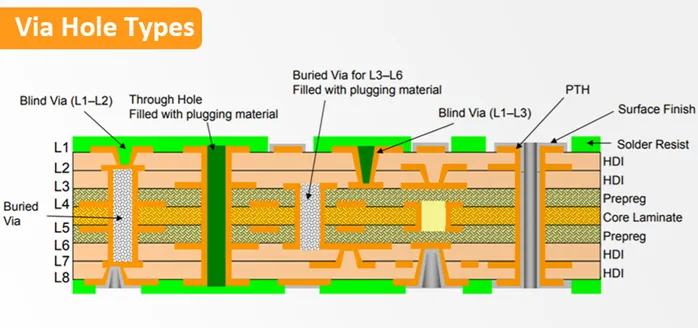
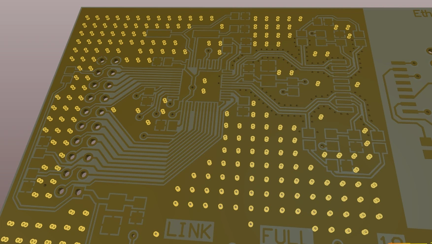
Buried vias are plated through-holes that interconnect two or more inner layers of a multilayer PCB, remaining completely hidden from the outer surfaces. Unlike through-hole vias, which span the entire board thickness, buried vias eliminate surface stubs that can radiate electromagnetic energy. This configuration proves essential in high-density boards where space constraints demand efficient routing. In the context of EMI, buried vias contribute to shielding techniques buried via by preserving continuous ground and power planes on outer layers. IPC-2221 provides guidelines for via design that emphasize such structures for controlled impedance and reduced discontinuities. Overall, buried vias enable denser layouts without compromising electromagnetic performance.
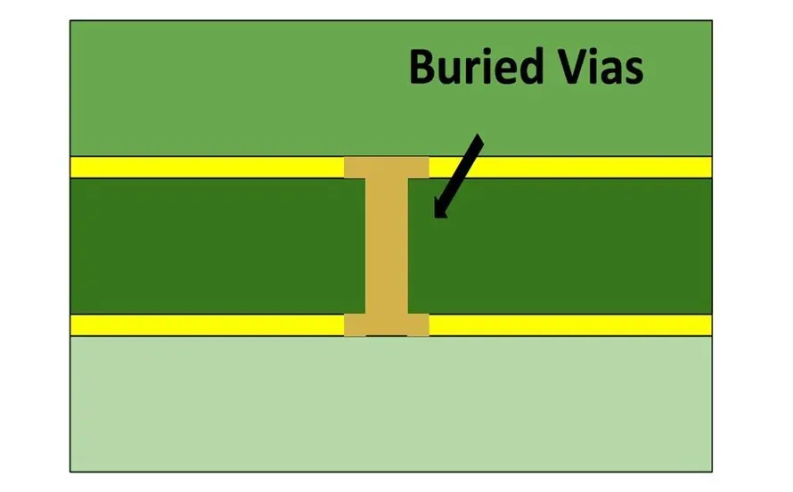
The distinction between buried, blind, and through vias influences EMI susceptibility. Blind vias connect an outer layer to an inner one, while buried vias operate solely internally. Engineers select buried vias when signals require transitions between non-adjacent inner layers, avoiding the EMI hotspots created by longer through vias. Manufacturing processes like sequential lamination support buried via fabrication, ensuring reliability under thermal stress. These vias align with performance specifications in IPC-6012E for rigid printed boards.
Mechanisms of EMI Generation in Vias
Vias introduce EMI primarily through impedance discontinuities and resonant stub effects. A through via's unused portion beyond the signal layer acts as a high-impedance stub, reflecting signals and radiating energy at frequencies where its length equals a quarter wavelength. This radiation couples to nearby traces or escapes the board enclosure, exacerbating electromagnetic interference PCB design issues. Return current paths also suffer interruptions around vias, creating large loop areas that amplify magnetic field emissions. Simulations reveal that stub lengths above certain thresholds correlate with peak EMI levels in the GHz range. Addressing these requires vias that maintain short, predictable electrical lengths.
Buried vias mitigate these issues by tailoring connections to exact layer spans. Without surface extensions, they eliminate radiating stubs entirely, confining fields within inner dielectrics. This containment reduces far-field emissions and improves near-field coupling control. Additionally, buried vias facilitate tighter plane partitioning, where ground planes sandwich signal layers for superior shielding. The result manifests as lower insertion loss and crosstalk, critical for buried via PCB EMI reduction.
How Buried Vias Enhance EMI Performance
Buried vias directly impact EMI by shortening the via structure's effective length, which lowers series inductance and shunt capacitance. Shorter vias exhibit less resonance, pushing problematic frequencies higher or damping them altogether. In high-speed designs, this preserves signal eye diagrams while curbing emissions. Ground return paths remain continuous across buried via transitions, minimizing loop inductance that drives differential-mode EMI. Empirical observations confirm that boards with buried vias show measurable drops in radiated emissions during compliance testing.
Shielding benefits emerge when buried vias integrate with via fencing or stitching arrays. Arrays of grounded buried vias form low-impedance barriers around sensitive traces, reflecting or absorbing plane waves. This technique enhances isolation between aggressor and victim nets, aligning with shielding techniques buried via principles. Layer stackups optimized for buried vias position power and ground planes adjacently to signals, creating Faraday cage-like enclosures. IPC-2226 outlines rules for such high-density interconnects, including via reliability under EMI-induced stresses.
The interplay between via type and dielectric materials further refines performance. Low-loss dielectrics around buried vias suppress surface waves that propagate EMI along planes. Engineers balance via aspect ratios to avoid plating voids, which could create EMI leaks. Comprehensive modeling verifies these gains before fabrication.
Best Practices for Buried Vias in EMI-Optimized Designs
Start with stackup planning to maximize buried via utility. Allocate inner layers for high-speed signals flanked by ground planes, using buried vias for transitions. Maintain via diameters under 10 mils for minimal parasitics, adhering to manufacturer drill capabilities. Space buried vias at least 3 times the diameter from adjacent features to prevent crosstalk. Simulate S-parameters to quantify EMI reductions, targeting return loss below -20 dB up to operating frequencies.
Incorporate via stitching liberally around buried signal vias. Stitch ground vias at lambda/20 spacing along plane edges and trace perimeters to bolster shielding. Combine buried vias with blind vias for hybrid structures in HDI boards, optimizing outer layer density. During layout, route signals orthogonally across layers to decouple fields. Post-layout checks verify no unshielded stubs remain.
Fabrication considerations ensure buried via integrity. Sequential build-up processes control depth precisely, avoiding misalignment that induces EMI hotspots. Thermal cycling tests per IPC standards confirm via stability under power-induced heating. Procurement specs should mandate filled or tented vias for added protection.
Advanced Integration and Troubleshooting
In RF and mixed-signal PCBs, buried vias excel in cavity filters or antenna feeds by isolating modes. Troubleshooting EMI spikes often traces to via-plane transitions; inspect for voids via cross-sectioning. If emissions persist, add moats around buried via clusters to sever surface currents. Field solvers help iterate stackups virtually.
Layer count influences efficacy: 8+ layer boards leverage multiple buried via pools for zoned shielding. Balance cost by limiting buried vias to critical nets.
Conclusion
Buried vias profoundly influence EMI performance by eliminating stubs, enhancing shielding, and preserving plane continuity. These structures enable buried via PCB EMI reduction essential for complying with electromagnetic interference PCB design demands. Best practices in stackup, placement, and integration yield robust results. Engineers applying shielding techniques buried via unlock higher densities without emission trade-offs. Prioritizing these in design workflows ensures reliable, high-performance PCBs.
FAQs
Q1: What is buried via PCB EMI reduction and how does it work?
A1: Buried via PCB EMI reduction involves using internal vias to connect layers without surface stubs, minimizing radiation from resonant lengths. These vias shorten electrical paths, reduce inductance, and maintain continuous return currents, lowering emissions. Ground planes adjacent to signal layers further contain fields. This aligns with high-speed design needs, improving compliance without added shielding layers.
Q2: How do buried vias contribute to electromagnetic interference PCB design improvements?
A2: Buried vias enhance electromagnetic interference PCB design by eliminating through-hole extensions that act as antennas. They support denser routing with lower crosstalk and better impedance control. Integrating them with stitching creates effective barriers. Simulations confirm reduced far-field radiation, vital for GHz signals. Follow IPC guidelines for optimal placement.
Q3: What shielding techniques buried via offer the best EMI mitigation?
A3: Shielding techniques buried via excel through via fencing and plane stitching, where arrays of grounded buried vias block waves. Position them lambda/20 apart around traces for isolation. Combine with orthogonal routing to decouple layers. This confines EMI within dielectrics, boosting immunity. Verify via thermal reliability in stackups.
Q4: When should engineers prioritize buried vias for EMI-sensitive PCBs?
A4: Prioritize buried vias in EMI-sensitive PCBs for speeds above 1 GHz or dense layouts needing plane integrity. They outperform through vias in multilayer boards by curbing stub radiation. Use when surface space limits stitching. Assess via cost against EMI test savings. Standards like IPC-2221 guide implementation.
References
IPC-2221B — Generic Standard on Printed Board Design. IPC, 2009
IPC-6012E — Qualification and Performance Specification for Rigid Printed Boards. IPC, 2017
IPC-2226 — Design Standard for High Density Interconnect (HDI). IPC, 2003