Introduction
Thick copper printed circuit boards (PCBs) are essential for high-power applications, such as power electronics, automotive systems, and industrial controls. These boards often feature copper layers exceeding 3 ounces per square foot, providing superior current-carrying capacity and thermal dissipation. However, the integration of solder mask on thick copper PCBs introduces unique challenges, including adhesion issues, cracking, and reliability concerns. Solder mask, a protective polymer layer, insulates copper traces and prevents solder bridges during assembly. With thicker copper, the interaction between the mask and the substrate becomes more complex, risking performance degradation. This article explores the impact of solder mask on thick copper PCBs, delving into technical challenges and offering practical solutions for engineers. Understanding these factors ensures enhanced reliability and longevity in demanding environments.
What Is Solder Mask and Its Role in Thick Copper PCBs
Solder mask is a thin, protective coating applied over the copper traces of a PCB to prevent oxidation and unintended solder connections during assembly. Typically composed of epoxy or acrylic-based polymers, it also provides insulation and protects against environmental factors like moisture and dust. In standard PCBs, solder mask application is straightforward, but thick copper PCBs present distinct challenges due to their unique physical and thermal properties.
In thick copper designs, the solder mask must withstand greater mechanical stress and thermal expansion differences between the copper and the substrate. The thicker copper layers, often used in high-current applications, generate more heat, which can strain the solder mask integrity. Reliability becomes a critical concern, as any failure in the mask layer can expose copper, leading to short circuits or corrosion. Ensuring proper adhesion and resistance to cracking is vital for maintaining the board's performance under operational stress. For engineers, recognizing the importance of solder mask in these contexts drives better design and manufacturing decisions.
Related Reading: Understanding Solder Mask: A Beginner's Guide to PCB Protection
Technical Challenges of Solder Mask on Thick Copper PCBs
Adhesion Issues
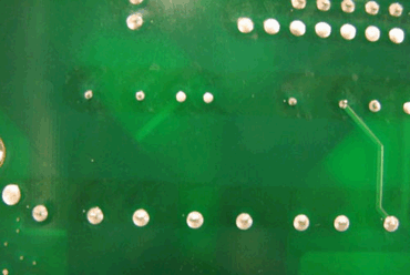
One of the primary challenges with solder mask on thick copper PCBs is achieving strong adhesion. The increased copper thickness creates a larger height differential between traces and the substrate, making it difficult for the mask to conform uniformly. Poor adhesion can result in delamination, where the mask peels away from the copper or substrate, exposing traces to environmental hazards. This issue often arises due to surface contamination, inadequate surface preparation, or mismatched thermal expansion coefficients between materials. If the solder mask fails to bond properly, the reliability of the PCB diminishes, especially in high-vibration or thermal cycling conditions.
Cracking Under Thermal Stress
Thick copper PCBs are frequently used in applications with significant heat generation, such as power supplies or motor controllers. The thermal expansion mismatch between the copper, substrate, and solder mask can induce stress, leading to cracking in the mask layer. Cracks compromise the protective barrier, allowing moisture or contaminants to reach the copper, which accelerates corrosion and potential failure. This challenge is exacerbated during reflow soldering processes, where rapid temperature changes test the material's durability. Ensuring the solder mask can endure these conditions without fracturing is a critical design consideration.
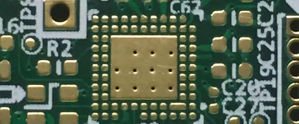
Uneven Application and Coverage
Applying solder mask evenly over thick copper layers poses another hurdle. The height variations between thick copper traces and the surrounding substrate can lead to incomplete coverage or thin spots in the mask layer. These inconsistencies increase the risk of exposed copper, undermining the board's reliability. Additionally, thick copper often requires wider traces or pads, which can complicate mask alignment and increase the likelihood of defects like pinholes or voids. Such flaws may not be immediately apparent but can cause long-term issues in harsh operating environments.
Impact on Reliability
The cumulative effect of adhesion problems, cracking, and uneven coverage directly impacts the reliability of thick copper PCBs. In high-power applications, where boards are subjected to extreme electrical and thermal loads, even minor solder mask failures can lead to catastrophic outcomes. Short circuits, insulation breakdown, and trace corrosion are common failure modes when the mask layer is compromised. For engineers, addressing these challenges is essential to meet industry standards like IPC-6012E, which outlines performance specifications for rigid printed boards.
Practical Solutions for Solder Mask Challenges on Thick Copper PCBs
Surface Preparation and Cleaning
Effective surface preparation is critical to improving solder mask adhesion on thick copper PCBs. Before application, the copper surface must be thoroughly cleaned to remove oxides, oils, and other contaminants. Micro-etching or mechanical abrasion can enhance surface roughness, providing a better bonding area for the mask. Following guidelines from standards like IPC-A-600K, which specifies acceptability criteria for printed boards, ensures that surface conditions meet necessary requirements. Proper cleaning minimizes the risk of delamination and boosts long-term reliability.
Material Selection for Solder Mask
Choosing the right solder mask material is vital for thick copper applications. High-performance masks with improved thermal and mechanical properties, such as those with higher glass transition temperatures, can better withstand the stresses associated with thick copper layers. Liquid photoimageable (LPI) solder masks are often preferred for their ability to conform to uneven surfaces, ensuring uniform coverage. Engineers should consult material datasheets and align selections with standards like IPC-SM-840E, which governs solder mask performance, to optimize compatibility with thick copper designs.
Optimized Application Techniques
The method of solder mask application significantly affects its performance on thick copper PCBs. Screen printing or curtain coating must be carefully controlled to achieve consistent thickness and coverage, especially over elevated copper traces. Adjusting process parameters, such as curing time and temperature, can prevent issues like incomplete curing or excessive brittleness, which contribute to cracking. Adhering to manufacturing guidelines ensures the mask layer remains intact during thermal cycling and operational stress.
Design Considerations for Stress Reduction
PCB design plays a pivotal role in mitigating solder mask challenges. Reducing sharp height transitions between copper traces and the substrate can improve mask conformity and reduce stress concentration points. Incorporating gradual trace profiles or adding dummy copper fills in non-critical areas can balance thermal expansion. Additionally, ensuring adequate solder mask clearance around pads, as recommended by IPC-2221B for generic PCB design, minimizes the risk of misalignment or insufficient coverage. Thoughtful design enhances both adhesion and overall reliability.
Thermal Management Strategies
Effective thermal management is essential to prevent solder mask cracking in thick copper PCBs. Using substrates with low coefficients of thermal expansion (CTE) reduces the mismatch between materials during temperature changes. Adding thermal vias or heat sinks near high-power components dissipates heat more evenly, lowering stress on the mask layer. Engineers should reference standards like IPC-7095D, which addresses design for ball grid arrays and thermal considerations, to integrate robust thermal solutions into their designs.
Troubleshooting Solder Mask Issues in Manufacturing
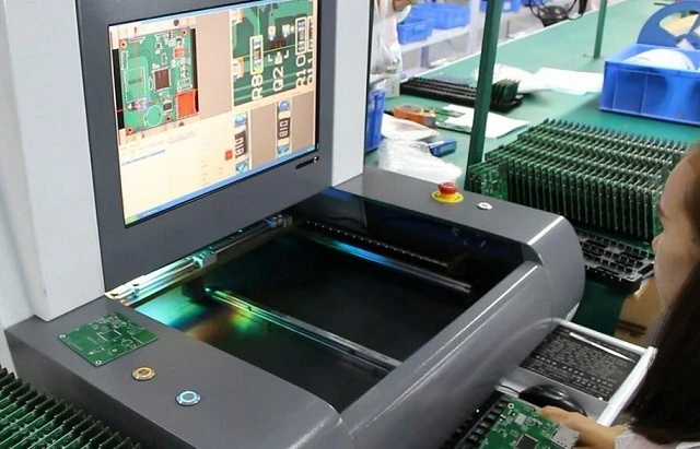
During manufacturing, identifying and addressing solder mask issues early can save significant time and cost. Visual inspection, as outlined in IPC-A-600K, helps detect defects like pinholes, cracks, or delamination before boards proceed to assembly. Advanced techniques, such as automated optical inspection (AOI), provide detailed analysis of mask coverage and alignment over thick copper traces. If adhesion problems are observed, revisiting surface preparation protocols or adjusting curing conditions may resolve the issue. For cracking, evaluating the thermal profile during reflow soldering ensures temperatures remain within safe limits for the chosen mask material. Consistent monitoring and adherence to industry standards prevent reliability issues in the final product.
Related Reading: Solder Mask Misalignment: Causes, Consequences, and Solutions for Robust PCB Production
Conclusion
Solder mask plays a crucial role in protecting thick copper PCBs, ensuring insulation, and maintaining reliability in high-power applications. However, challenges like adhesion difficulties, cracking under thermal stress, and uneven application can compromise performance if not addressed. By focusing on proper surface preparation, selecting suitable materials, optimizing application techniques, and incorporating thoughtful design and thermal management strategies, engineers can overcome these obstacles. Adhering to recognized standards, such as those from IPC, provides a solid foundation for achieving durable and reliable solder mask performance. With these solutions, thick copper PCBs can meet the stringent demands of modern electronics, delivering consistent operation in challenging environments.
FAQs
Q1: How does solder mask adhesion affect thick copper PCB performance?
A1: Solder mask adhesion is critical for thick copper PCB performance. Poor bonding can lead to delamination, exposing copper traces to moisture and contaminants, which causes corrosion or short circuits. This reduces reliability, especially in high-power applications with thermal and mechanical stress. Proper surface preparation and material selection, aligned with industry standards, ensure strong adhesion and protect the board over its operational life. - Sophia Wang, Manufacturing Specialist
Q2: What causes solder mask cracking on thick copper PCBs?
A2: Solder mask cracking on thick copper PCBs often results from thermal expansion mismatches between the copper, substrate, and mask during temperature changes. High heat in power applications or reflow soldering exacerbates stress, leading to fractures. Selecting masks with high thermal tolerance and implementing thermal management solutions, like vias, can mitigate this issue effectively. - Sophia Wang, Manufacturing Specialist
Q3: How can reliability be improved for thick copper PCBs with solder mask?
A3: Improving reliability for thick copper PCBs involves optimizing solder mask application, ensuring proper adhesion, and preventing cracking. Use high-quality materials, clean surfaces thoroughly, and design for thermal balance. Following standards like IPC-6012E for performance specifications helps maintain consistent quality. Regular inspections during manufacturing also catch defects early, ensuring long-term durability in demanding conditions. - Sophia Wang, Manufacturing Specialist
Q4: What design tips help with solder mask on thick copper PCBs?
A4: For thick copper PCBs, design tips include minimizing height transitions between traces and substrate to improve solder mask coverage. Add dummy copper fills for thermal balance and ensure adequate mask clearance around pads per IPC-2221B guidelines. These steps reduce stress points, enhance adhesion, and prevent cracking, contributing to overall board reliability in high-power setups. - Sophia Wang, Manufacturing Specialist
References
IPC-6012E — Qualification and Performance Specification for Rigid Printed Boards. IPC, 2020.
IPC-A-600K — Acceptability of Printed Boards. IPC, 2020.
IPC-SM-840E — Qualification and Performance of Permanent Solder Mask and Flexible Cover Materials. IPC, 2010.
IPC-2221B — Generic Standard on Printed Board Design. IPC, 2012.
IPC-7095D — Design and Assembly Process Implementation for Ball Grid Arrays (BGAs). IPC, 2018.


