Introduction
In the realm of printed circuit board design, achieving precise impedance control is a cornerstone for ensuring optimal performance, especially in high-frequency applications. One critical factor that directly influences impedance is PCB laminate thickness. This parameter, often overlooked in initial design stages, plays a pivotal role in maintaining signal integrity and meeting stringent electrical requirements. For electrical engineers, understanding how laminate thickness interacts with dielectric properties and impedance calculation is essential to prevent signal degradation and ensure reliable operation. This article explores the significance of laminate thickness in high-frequency PCB design, delving into its impact on impedance control and offering practical guidance for achieving desired outcomes. By focusing on fundamental principles and industry standards, we aim to provide a comprehensive resource for designing robust and efficient circuit boards.
What Is PCB Laminate Thickness and Why It Matters
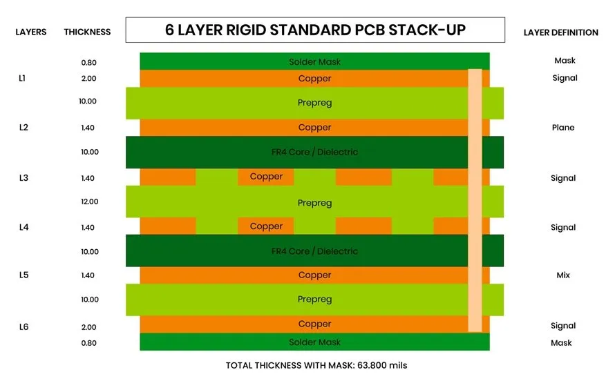
PCB laminate thickness refers to the measurement of the dielectric material layer sandwiched between conductive copper layers in a printed circuit board. This thickness varies depending on the design requirements, material selection, and intended application, typically ranging from a few mils to thicker dimensions in multilayer boards. It serves as the insulating barrier that influences electrical characteristics, including capacitance and impedance.
The importance of laminate thickness becomes evident in designs of the high frequency PCB, where signal integrity is paramount. Variations in thickness can alter the dielectric properties, affecting how signals propagate through transmission lines. Inconsistent thickness may lead to impedance mismatches, resulting in reflections, crosstalk, or signal loss. For engineers working on applications like telecommunications or RF systems, controlling this parameter ensures that the board meets performance specifications and maintains reliability under demanding conditions.
Technical Principles of Laminate Thickness in Impedance Control
Relationship Between Laminate Thickness and Impedance Calculation
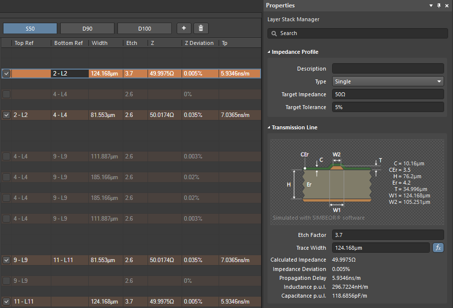
Impedance in a PCB is determined by several factors, including trace width, trace spacing, dielectric constant of the material, and laminate thickness. In a microstrip or stripline configuration, the thickness of the dielectric layer directly impacts the characteristic impedance of the transmission line. A thinner laminate reduces the distance between the signal trace and the reference plane, typically lowering the impedance. Conversely, a thicker laminate increases this distance, raising the impedance value.
This relationship is critical during impedance calculation, as even minor deviations in laminate thickness can cause significant shifts in the expected impedance. For high-frequency PCB design, where tight tolerances are necessary, engineers must account for manufacturing variations in laminate thickness to avoid performance issues. Industry standards, such as IPC-2141A, provide guidelines for controlled impedance design, emphasizing the need for precise thickness specifications in the design phase.
Dielectric Properties and Their Influence
Dielectric properties, particularly the dielectric constant and loss tangent of the laminate material, interact closely with laminate thickness. The dielectric constant determines how much electric field is stored in the material, affecting signal speed and impedance. A consistent thickness ensures that the dielectric behavior remains uniform across the board. Variations can lead to localized changes in signal propagation, undermining signal integrity.
In high-frequency applications, materials with low dielectric constants are often preferred to minimize signal delay. However, if the laminate thickness is not uniform, even the best materials cannot guarantee performance. Engineers must balance material selection with precise thickness control to achieve the desired electrical characteristics.
Impact on Signal Integrity in High-Frequency Designs
Signal integrity is a primary concern in high-frequency PCB design, where fast-switching signals are prone to distortion. Laminate thickness variations can introduce impedance discontinuities, leading to signal reflections that degrade performance. These reflections may cause data errors or complete signal failure in critical systems like 5G infrastructure or high-speed digital circuits.
Additionally, uneven thickness can contribute to crosstalk between adjacent traces, as the electromagnetic fields interact unpredictably. Maintaining a uniform laminate thickness mitigates these risks, ensuring that signals travel with minimal interference. Adhering to standards like IPC-6012E for rigid board performance helps engineers specify acceptable tolerances for laminate thickness, safeguarding signal integrity.
Practical Solutions for Controlling Laminate Thickness
Design Considerations for Impedance Control
During the design phase, engineers should define laminate thickness based on the target impedance and application requirements. Using simulation tools aligned with industry standards, such as IPC-2141A, allows for accurate impedance calculation before fabrication begins. Specifying tight tolerances for laminate thickness in the design documentation ensures that manufacturers understand the critical nature of this parameter.
Selecting the appropriate dielectric material is equally important. Materials with stable dielectric properties across different thicknesses provide consistency in high-frequency PCB design. Engineers should consult material datasheets and adhere to guidelines in IPC-4101E for laminate specifications to match thickness with electrical performance goals.
Manufacturing Tolerances and Quality Control
Manufacturing processes must align with design specifications to maintain laminate thickness within acceptable limits. Standards like IPC-A-600K outline acceptability criteria for printed boards, including tolerances for dielectric layers. Engineers should collaborate with fabrication teams to verify that lamination processes achieve uniform thickness across the board.
Quality control measures, such as cross-sectional analysis and thickness measurement during production, help identify deviations early. Implementing inspection protocols based on IPC-6012E ensures that the final product meets performance requirements. Consistency in manufacturing directly translates to reliable impedance control and signal integrity in the finished fast turn PCB.
Testing and Validation Techniques
Post-fabrication testing is essential to confirm that laminate thickness aligns with design intent. Techniques like time-domain reflectometry can detect impedance mismatches caused by thickness variations. Additionally, cross-sectional microscopy provides a direct view of the dielectric layer, verifying its uniformity.
Engineers should reference IPC-TM-650 for standardized test methods to evaluate dielectric properties and thickness. These tests validate that the PCB performs as expected under operational conditions, particularly in high-frequency applications. Regular validation builds confidence in the design and manufacturing process, reducing the risk of field failures.
Insights into High-Frequency PCB Design Challenges
High-frequency PCB design often involves balancing multiple constraints, with laminate thickness being a critical variable. In applications like RF circuits, even small deviations can disrupt signal paths, leading to costly redesigns. A common challenge is the natural variation in laminate materials during production, which can introduce inconsistencies.
To address this, engineers can specify prepreg and core materials with tight thickness tolerances as per IPC-4101E guidelines. Additionally, designing with margin for manufacturing variations helps accommodate minor discrepancies without compromising impedance control. Understanding the interplay between laminate thickness, dielectric properties, and signal integrity equips engineers to tackle these challenges effectively.
Conclusion
Laminate thickness stands as a fundamental element in achieving precise impedance control in printed circuit boards. Its influence on impedance calculation, dielectric properties, and signal integrity cannot be overstated, particularly in high-frequency PCB design. By understanding the technical principles and implementing practical solutions, electrical engineers can mitigate risks associated with thickness variations. Adherence to industry standards ensures that designs meet performance expectations, delivering reliable and efficient circuit boards. As technology advances, maintaining control over laminate thickness will remain a key factor in pushing the boundaries of PCB performance.
FAQs
Q1: How does PCB laminate thickness affect impedance control?
A1: PCB laminate thickness directly impacts impedance by altering the distance between signal traces and reference planes. A thinner laminate typically lowers impedance, while a thicker one increases it. For precise impedance control, maintaining uniform thickness is crucial to avoid mismatches that degrade signal integrity. Engineers must specify tight tolerances during design, following standards like IPC-2141A, to ensure consistent electrical performance across the board.
Q2: Why is signal integrity important in high-frequency PCB design?
A2: Signal integrity ensures that high-frequency signals transmit without distortion or loss, which is vital for applications like telecommunications. Laminate thickness variations can cause impedance discontinuities, leading to reflections and crosstalk. Maintaining uniform thickness and stable dielectric properties helps preserve signal quality. Adhering to standards such as IPC-6012E supports reliable performance under demanding conditions in high-frequency environments.
Q3: What role do dielectric properties play in impedance calculation?
A3: Dielectric properties, like the dielectric constant, determine how electric fields interact within the PCB material, affecting impedance calculation. Laminate thickness influences how these properties manifest in signal propagation. Consistent thickness ensures uniform dielectric behavior, preventing localized impedance shifts. Following guidelines in IPC-4101E for material selection aids engineers in achieving accurate impedance control for optimal board performance.
Q4: How can engineers ensure uniform laminate thickness in manufacturing?
A4: Engineers can ensure uniform laminate thickness by specifying tight tolerances in design documentation and collaborating with fabrication teams. Implementing quality control measures, such as cross-sectional analysis, during production helps detect variations. Adhering to standards like IPC-A-600K for acceptability criteria and IPC-6012E for performance specifications ensures that manufacturing processes align with design intent for reliable impedance control.
References
IPC-2141A — Design Guide for High-Speed Controlled Impedance Circuit Boards. IPC, 2004.
IPC-4101E — Specification for Base Materials for Rigid and Multilayer Printed Boards. IPC, 2021.
IPC-6012E — Qualification and Performance Specification for Rigid Printed Boards. IPC, 2020.
IPC-A-600K — Acceptability of Printed Boards. IPC, 2020.
IPC-TM-650 — Test Methods Manual. IPC, Current Revision.


