Introduction
In the realm of PCB prototyping, achieving cost efficiency without compromising quality remains a primary concern for electrical engineers. The size of a printed circuit board directly impacts manufacturing costs, material usage, and turnaround times, especially during rapid prototyping and quick turn cycles. Striking the right balance in PCB design ensures that projects stay within budget while meeting technical requirements. This article explores the optimal PCB size for cost-effective prototyping, delving into the factors that influence PCB cost and offering practical insights for engineers. By understanding the interplay between dimensions, production constraints, and design principles, professionals can streamline their workflow and enhance project outcomes. The focus here is on actionable strategies that align with industry standards to support efficient and economical PCB prototyping processes.
What Is PCB Prototyping and Why It Matters
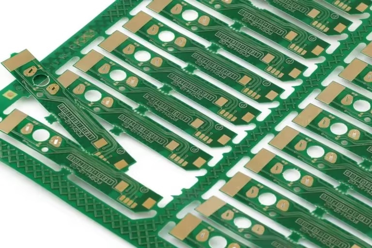
PCB prototyping involves creating initial versions of a printed circuit board to test and validate a design before full-scale production. This step is crucial for identifying flaws, ensuring functionality, and refining the layout to meet performance goals. For electrical engineers, prototyping serves as a bridge between conceptual design and market-ready products. It allows for iterative testing, which is essential in complex projects where errors can lead to significant delays or expenses. The cost of prototyping, often termed PCB cost, varies based on factors like board size, layer count, and turnaround time. Rapid prototyping and quick turn services further accelerate this process, enabling faster iterations. By prioritizing efficient rapid PCB prototyping, engineers can reduce development timelines, minimize risks, and ensure that the final product adheres to stringent quality and reliability standards.
Technical Principles Behind PCB Size and Cost
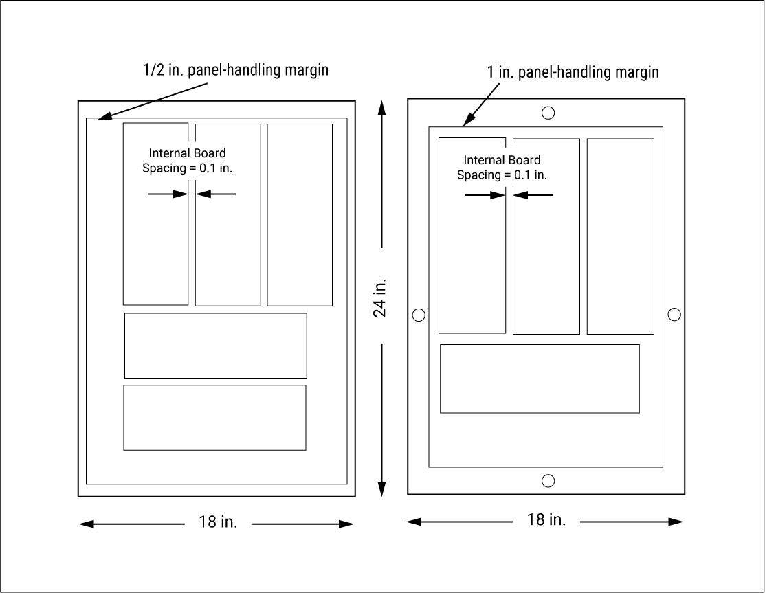
The dimensions of a PCB play a critical role in determining manufacturing expenses during prototyping. Larger boards require more raw materials, such as copper-clad laminates, and consume additional resources in terms of machine time and handling. Most production facilities operate within specific size constraints due to equipment limitations, often defined by panel sizes used in batch processing. Standard panel sizes, typically around 18 by 24 inches or smaller, dictate how many individual boards can be fabricated from a single sheet. If a PCB design exceeds these dimensions, it may necessitate custom paneling, which increases PCB cost significantly.
Beyond material costs, larger boards often complicate the manufacturing process. They may require specialized handling to prevent warpage or damage, as outlined in standards like IPC-6012E for rigid printed boards. Warpage can affect component placement accuracy and soldering reliability, leading to potential defects. Additionally, larger PCBs can pose challenges in maintaining uniform etching and plating across the surface, impacting trace integrity. These factors collectively elevate production expenses, especially in rapid prototyping scenarios where precision and speed are paramount.
Another key consideration is the yield rate. Smaller PCBs allow for higher panel utilization, meaning more units can fit into a single production run, reducing waste. Conversely, oversized designs may result in inefficient panel layouts, driving up costs per unit. Electrical engineers must also account for shipping and handling expenses, as larger boards often require custom packaging to prevent damage during transit. Balancing these technical constraints with project needs is essential for cost-effective PCB prototyping.
Factors Influencing PCB Cost in Prototyping
Several elements contribute to the overall PCB cost during prototyping, with size being a primary driver. Below are the key factors that electrical engineers should consider when aiming for cost efficiency:
- Board Dimensions: As previously mentioned, larger PCBs consume more material and may require non-standard processing, increasing expenses. Staying within common size ranges, such as 100 by 100 millimeters for prototypes, often yields better pricing.
- Layer Count: More layers mean higher complexity and cost. While size directly affects material usage, combining it with minimal layers can optimize expenses.
- Turnaround Time: Rapid prototyping and quick turn services prioritize speed, often at a premium. Smaller boards typically process faster due to easier handling and panel fitting, reducing costs in quick turn scenarios.
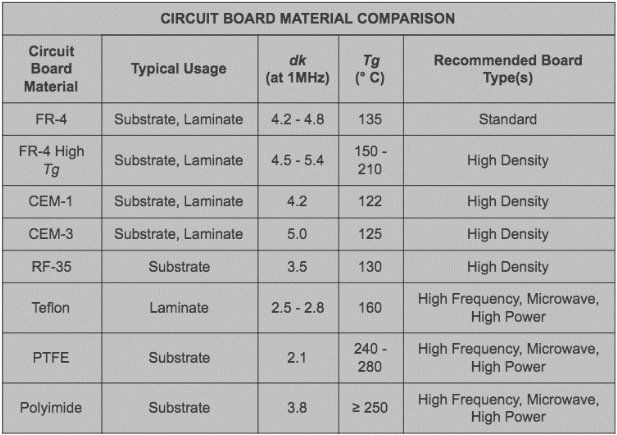
- Material Selection: Standard materials, like FR-4, are cost-effective for most prototypes. Larger boards using specialty materials for high-frequency applications can significantly raise expenses.
- Design Complexity: Dense layouts or intricate routing on larger boards may lead to longer production times and higher error rates, impacting cost.
Understanding these factors allows engineers to make informed decisions during PCB design. Adhering to industry guidelines, such as those in IPC-A-600K for printed board acceptability, ensures that designs remain manufacturable without unnecessary cost spikes.
Finding the Sweet Spot for PCB Size in Prototyping
Determining the optimal PCB size for cost-effective prototyping requires a strategic approach. Electrical engineers often aim for dimensions that maximize panel utilization while meeting project specifications. A common sweet spot for prototypes lies between 50 by 50 millimeters and 150 by 150 millimeters. Boards within this range typically fit well into standard manufacturing panels, minimizing material waste and reducing PCB cost. This size also simplifies handling, testing, and assembly, which is vital for rapid prototyping cycles.
For projects requiring larger boards, consider modular designs. Breaking a large PCB into smaller, interconnected sections can lower production expenses by aligning with standard panel sizes. This approach also facilitates easier troubleshooting and iterative testing, as individual modules can be modified without redesigning the entire board. Such strategies align with best practices for efficient PCB design, ensuring that functionality is not sacrificed for cost savings.
Additionally, engineers should consult manufacturing constraints early in the design phase. Many facilities provide guidelines on maximum and minimum board sizes for cost-effective processing. Staying within these limits avoids custom setups that inflate expenses, especially in quick turn scenarios. By prioritizing compact yet functional layouts, professionals can achieve a balance between performance and affordability during PCB prototyping.
Practical Best Practices for Cost-Effective PCB Design
To optimize PCB prototyping costs while maintaining quality, electrical engineers can adopt the following practices during the design and planning stages:
- Minimize Board Size: Focus on compact layouts by optimizing component placement and routing. Smaller boards reduce material usage and fit better into standard panels.
- Standardize Dimensions: Use common sizes that align with manufacturing capabilities to avoid custom paneling fees. Confirm acceptable dimensions with production guidelines.
- Leverage Design Rules: Follow industry standards like IPC-6012E to ensure manufacturability. This reduces the risk of defects that could necessitate costly redesigns.
- Plan for Iterations: In rapid prototyping, anticipate multiple revisions. Design with flexibility to adjust layouts without significant cost increases.
- Optimize Layer Usage: Limit the number of layers unless necessary for functionality. Fewer layers lower production complexity and expenses.
Implementing these practices during PCB design not only curbs costs but also enhances reliability. Engineers should also prioritize clear documentation and design reviews to catch potential issues before fabrication, saving time and resources in quick turn projects.
Insight into Balancing Size and Functionality
While minimizing PCB size is often ideal for cost savings, functionality must never be compromised. Electrical engineers frequently face the challenge of fitting complex circuits into limited space without sacrificing performance. For instance, in high-density designs, shrinking the board size might lead to thermal issues or signal interference if not carefully managed. Standards like IPC-6012E provide guidance on acceptable tolerances for trace widths and spacing, which are critical in compact layouts.
One effective strategy is to prioritize critical components and allocate space based on their requirements. Power management circuits, for example, may need additional clearance for heat dissipation, while high-speed signals require controlled impedance paths. Simulation tools can help predict potential issues in smaller designs, allowing for adjustments before prototyping. By iteratively refining the layout, engineers can achieve an optimal balance between size, cost, and performance, ensuring that the PCB meets all operational needs.
Conclusion
Achieving cost-effective PCB prototyping hinges on selecting the right board size and adhering to sound design principles. By targeting dimensions that align with standard manufacturing panels, electrical engineers can significantly reduce PCB cost while maintaining quality. Practical strategies, such as compact layouts, modular designs, and adherence to industry standards like IPC-6012E and IPC-A-600K, further enhance efficiency in rapid prototyping and quick turn projects. Balancing size with functionality ensures that performance remains uncompromised, even within tight budget constraints. Through careful planning and iterative testing, professionals can streamline their PCB design processes, paving the way for successful product development and innovation in the electronics field.
FAQs
Q1: What factors most impact PCB cost in PCB prototyping?
A1: The primary factors affecting PCB cost include board size, layer count, material type, and turnaround time. Larger boards use more materials and may require custom processing, increasing expenses. Rapid prototyping services often come at a premium, while complex designs with multiple layers add to production costs. Following standard sizes and minimizing complexity can help manage expenses effectively.
Q2: How does PCB size affect rapid prototyping timelines?
A2: PCB size directly influences rapid prototyping timelines due to manufacturing and handling constraints. Smaller boards fit efficiently into standard panels, speeding up fabrication and reducing setup times. Larger boards may need custom paneling or additional processing steps, delaying quick turn cycles. Optimizing size ensures faster iterations without compromising on design needs.
Q3: What are key considerations in PCB design for cost efficiency?
A3: In PCB design, cost efficiency depends on minimizing board size, reducing layer count, and adhering to manufacturing standards like IPC-6012E. Using standard dimensions avoids custom fees, while compact layouts lower material usage. Planning for iterative testing and avoiding overly complex routing also helps keep expenses in check during prototyping.
Q4: Why is quick turn prototyping important for engineers?
A4: Quick turn prototyping is vital for engineers as it accelerates the design validation process. Faster turnaround times allow for rapid iterations, helping identify and fix issues early. This reduces overall development timelines and ensures projects stay on schedule. Efficient PCB design practices further enhance the benefits of quick turn services for timely results.
References
IPC-6012E - Qualification and Performance Specification for Rigid Printed Boards. IPC, 2020.
IPC-A-600K - Acceptability of Printed Boards. IPC, 2020.


