Introduction
In printed circuit board design, minimum trace spacing stands as a critical parameter that directly influences the reliability and performance of electronic assemblies. Engineers often overlook the subtle interplay between trace proximity and electrical behavior, leading to issues like signal degradation and outright failures. This guide delves into the principles of pcb trace spacing failure analysis, highlighting how proper spacing safeguards against common pitfalls. By understanding signal integrity trace spacing requirements, designers can optimize layouts for high-speed applications and long-term durability. The discussion draws on established engineering practices to provide actionable insights for electric engineers tackling complex PCB projects. Ultimately, mastering minimum trace spacing elevates design quality while minimizing manufacturing risks.
What Is Minimum Trace Spacing and Why It Matters
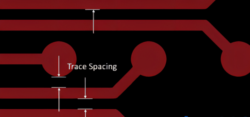
Minimum trace spacing refers to the smallest allowable distance between conductive elements on a PCB, such as traces, pads, or vias, measured edge-to-edge. This parameter ensures mechanical separation during fabrication and assembly, while also addressing electrical isolation needs. In high-density boards, insufficient spacing compromises manufacturability, as etching processes demand clear differentiation between features. From an electrical standpoint, it prevents unintended coupling that could distort signals or cause arcing under voltage stress. Adhering to minimum trace spacing for impedance control becomes essential in high-frequency designs, where trace geometry dictates characteristic impedance. Neglecting these guidelines results in elevated failure rates, underscoring their relevance across industries from consumer electronics to aerospace.
The importance amplifies in modern applications with rising clock speeds and power densities. Close traces exacerbate electromagnetic interference, leading to the effects of insufficient trace spacing such as increased crosstalk and ground bounce. During pcb trace spacing failure analysis, engineers frequently identify spacing violations as root causes of intermittent issues. Proper spacing aligns with design rules that balance board real estate with performance margins. It also facilitates compliance with fabrication capabilities, reducing yield losses. For electric engineers, integrating these considerations early in the layout phase prevents costly redesigns.
Technical Principles Behind Trace Spacing
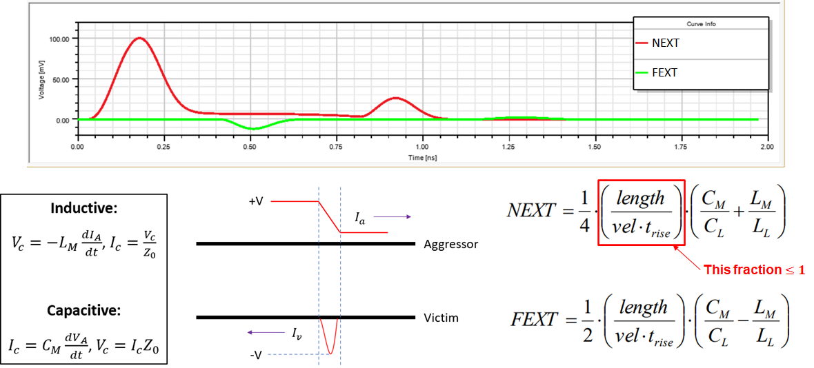
Trace spacing governs multiple physical phenomena in PCB operation. Capacitive coupling arises when adjacent traces form unintended capacitors, allowing noise transfer between signals. Inductive coupling similarly induces voltage spikes via mutual inductance, particularly in parallel runs. These effects intensify with proximity, frequency, and rise times, degrading signal integrity trace spacing thresholds. In multilayer boards, interlayer spacing must account for via stub interactions and plane proximity. Engineers model these using field solvers to predict coupling coefficients and adjust layouts accordingly.
For voltage isolation, spacing prevents dielectric breakdown and surface tracking. Higher potentials demand greater distances to withstand electric fields without flashover. IPC-2221 outlines requirements for conductor spacing based on operating voltage and environmental factors, distinguishing between external and internal conductors. Fabrication tolerances further influence effective spacing, as etch undercut can encroach on nominal gaps. Thermal expansion during operation may also alter distances, emphasizing conservative margins. These principles form the foundation for robust designs resistant to environmental stresses.
Impedance control relies heavily on consistent trace spacing relative to reference planes. In microstrip configurations, adjacent trace spacing affects coupling impedance, altering differential pair performance. Stripline designs require uniform spacing to ground planes for predictable characteristic impedance. Variations introduce reflections, causing overshoot and ringing. Minimum trace spacing for impedance control thus integrates with width and stackup definitions. Simulations validate these parameters, ensuring eye diagram margins meet specifications.
Effects of Insufficient Trace Spacing
The effects of insufficient trace spacing manifest across electrical, thermal, and mechanical domains. Electrically, crosstalk dominates high-speed scenarios, where forward and backward coupling corrupts data eyes. This leads to bit error rates climbing exponentially with reduced spacing. In power distribution networks, tight spacing elevates IR drop and voltage gradients, risking hot spots. Signal integrity trace spacing violations often trigger compliance failures in validation testing.
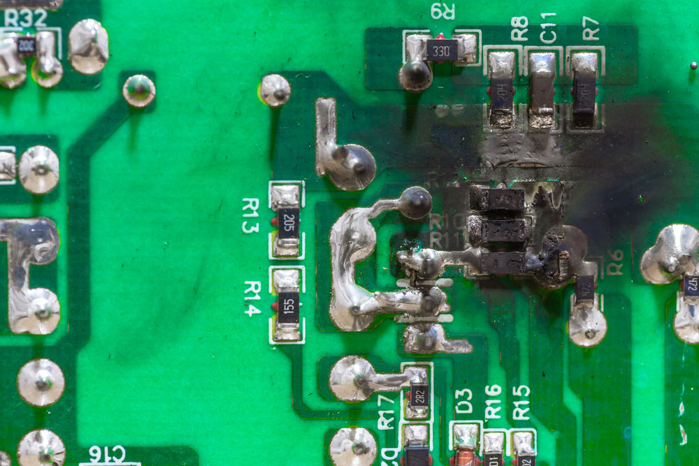
Mechanically, narrow gaps heighten shorting risks from solder bridges or debris during assembly. Etch defects like mouse bites or over-etching bridge traces, evident in pcb trace spacing failure analysis via cross-sectioning. High-voltage applications face creepage and clearance failures, promoting arcing paths along surfaces. Cumulative effects include accelerated electromigration in copper, shortening lifespan. Thermal crosstalk compounds issues, as heat from one trace influences neighbors' resistance.
Failure modes escalate under stress testing. Humidity accelerates dendritic growth across underspaced traces, forming conductive filaments. Vibration induces fretting corrosion at edges. IPC-A-600 provides acceptability criteria for conductor spacing, aiding visual inspections post-fabrication. These insights guide root cause analysis, revealing patterns like batch-specific etch biases.
Practical Solutions and Best Practices
Engineers should establish design rules enforcing minimum trace spacing from project outset. Start with stackup planning to define layer-specific gaps, incorporating fab supplier feedback. For high-speed nets, apply spacing at least three times the trace width to suppress coupling. Route critical signals on inner layers with ground shielding, maximizing isolation. Verify impedance targets through field solvers integrated in layout tools.
During routing, prioritize orthogonal paths to minimize parallel lengths. Use guard traces or stitching vias to interrupt coupling paths. For power and ground, allocate wider clearances to mitigate arcing. Simulate signal integrity trace spacing scenarios, iterating on eye patterns and jitter budgets. Post-layout, run design rule checks flagging violations.
Fabrication handoff demands clear documentation of spacing rules. Specify class levels per IPC-6012 for performance qualification. DFM reviews assess etch factor impacts on gaps. Assembly processes benefit from stencil apertures avoiding paste bridging. Field returns inform iterative refinements, closing the feedback loop.
Troubleshooting PCB Trace Spacing Failures
Pcb trace spacing failure analysis begins with symptom categorization: intermittent vs. hard fails, thermal dependency, or speed-related. Electrical testing isolates shorts via flying probe or bed-of-nails fixtures. Visual aids like optical microscopy reveal etch anomalies. Cross-section polishing exposes layer alignments and gap integrity.
Advanced techniques employ X-ray for buried defects and thermal imaging for hot spots. Time-domain reflectometry pinpoints impedance discontinuities from spacing errors. Failure modes link back to design rules, prompting stackup revisions. Documentation of analysis feeds into continuous improvement.
Conclusion
Minimum trace spacing remains a cornerstone of reliable PCB design, intertwining signal integrity, manufacturability, and longevity. By grasping the effects of insufficient trace spacing and leveraging standards like IPC-2221, engineers mitigate risks proactively. Best practices in routing, simulation, and analysis ensure compliance and performance. This holistic approach not only prevents failures but optimizes board efficiency. Electric engineers armed with these strategies deliver robust solutions across demanding applications.
FAQs
Q1: What are the primary causes identified in pcb trace spacing failure analysis?
A1: Pcb trace spacing failure analysis commonly uncovers causes like etch over-etching, solder bridging, and dendritic growth under humidity. Capacitive coupling from tight layouts induces crosstalk, failing signal margins. Mechanical stresses exacerbate gaps, leading to frets. Standards guide thresholds, while cross-sectioning confirms defects. Addressing via DFM prevents recurrence.
Q2: How does signal integrity trace spacing impact high-speed designs?
A2: Signal integrity trace spacing dictates crosstalk levels and impedance uniformity in high-speed PCBs. Closer traces amplify coupling, distorting eye diagrams and increasing jitter. The 3W rule offers a practical minimum for isolation. Simulations quantify effects, guiding adjustments. Proper spacing preserves data rates and reduces EMI.
Q3: Why is minimum trace spacing for impedance control critical in multilayer boards?
A3: Minimum trace spacing for impedance control ensures consistent characteristic impedance across coupled lines and reference planes. Variations cause reflections and signal skew in differential pairs. Stackup symmetry relies on uniform gaps. Field solvers validate targets pre-fabrication. This maintains timing budgets in RF applications.
Q4: What are the main effects of insufficient trace spacing during operation?
A4: Effects of insufficient trace spacing include heightened crosstalk, arcing risks, and thermal runaway. Noise couples into signals, elevating BER. High voltage stresses provoke breakdown. Assembly defects like bridges cause immediate shorts. Long-term, migration accelerates. Analysis per IPC criteria isolates issues effectively.
References
IPC-2221 — Generic Standard on Printed Board Design. IPC
IPC-A-600 — Acceptability of Printed Boards. IPC
IPC-6012 — Qualification and Performance Specification for Rigid Printed Boards. IPC


