Introduction
Non-plated through-hole (NPTH) technology plays a crucial role in modern PCB fabrication, offering engineers a reliable option for mechanical features without the need for electrical conductivity. These holes pass completely through the board but lack the copper plating found in plated through-holes (PTH), making them ideal for applications like mounting and alignment. In high-volume production, incorporating NPTH design guidelines early can optimize both performance and manufacturability. This guide explores the fundamentals of NPTH, from design considerations to the manufacturing process, helping electrical engineers make informed decisions for their projects. By understanding NPTH applications and cost implications, teams can balance functionality with efficiency in PCB fabrication.
What Is Non-Plated Through-Hole Technology and Why Does It Matter?
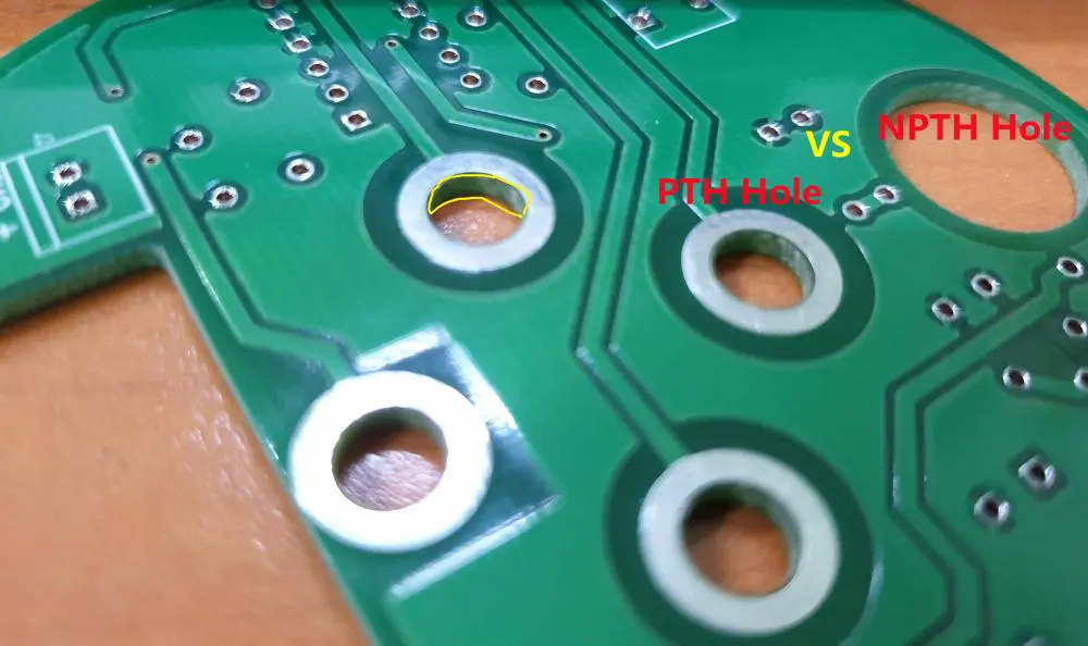
NPTH refers to holes drilled through all layers of a printed circuit board without any metallization on the walls, distinguishing them from PTH which feature copper plating for interlayer connections. This absence of plating simplifies fabrication and reduces costs, as no electroless or electrolytic processes are required for these features. NPTH serves primarily mechanical purposes, such as accommodating screws, pins, or standoffs for chassis mounting, or providing fiducial marks for assembly alignment.
The relevance of NPTH in PCB fabrication stems from its versatility in designs where electrical vias are unnecessary. For instance, vent holes allow gas escape during soldering to prevent delamination, enhancing board reliability. In cost-sensitive projects, using NPTH over PTH for non-conductive needs lowers material and processing expenses significantly. Electrical engineers value NPTH for maintaining signal integrity, as these holes do not introduce capacitance or inductance like plated vias might.
Adopting NPTH aligns with industry standards like IPC-A-600, which outlines acceptability criteria for such features in production boards. Overall, NPTH technology supports compact, robust designs in sectors ranging from consumer electronics to industrial controls.
Technical Principles of NPTH in PCB Design
The core principle of NPTH revolves around precise drilling to create clean, dimensionally stable holes without subsequent plating. Engineers must consider board thickness, material properties, and drill bit capabilities when specifying NPTH. Hole walls remain insulated by the base laminate, preventing short circuits if components press against them.
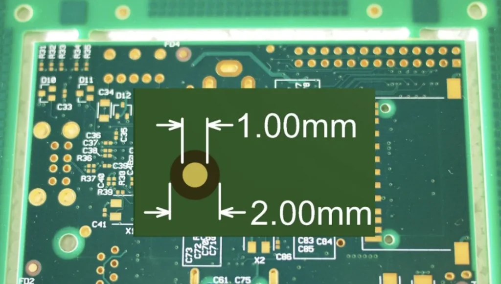
NPTH design guidelines emphasize minimum diameters and spacing to ensure manufacturability. Typical minimum sizes accommodate standard tooling, while clearances from copper traces prevent drill wander or breakout. Landed NPTH include pads for mechanical support, whereas landless versions save space in dense layouts. Aspect ratios, defined as board thickness to hole diameter, influence drill quality, with higher ratios risking rough walls or misalignment.
In multilayer boards, NPTH positioning avoids interfering with inner layer routing. Tolerances for NPTH are often tighter than for PTH due to the lack of plating forgiveness, as specified in IPC-6012 for rigid board performance. Engineers should simulate drill breakout on outer layers to predict fab yields.
NPTH Design Guidelines for Electrical Engineers
Effective NPTH design guidelines start with defining hole sizes based on component requirements, such as screw diameters plus clearance for insertion. Annular rings, if used, provide solder or adhesive bonding surfaces, but oversized pads increase copper waste. Minimum edge-to-hole distances prevent cracking during depaneling or thermal stress.
Spacing between NPTH and adjacent features maintains structural integrity. For fiducials, NPTH placement at board corners aids pick-and-place accuracy without electrical impact. In high-frequency designs, NPTH locations minimize ground plane interruptions.
Fabrication drawings must clearly distinguish NPTH from PTH using drill files, specifying tolerances per class. Compliance with IPC-A-600 ensures visual and dimensional acceptability post-drill. Testing prototypes verifies fit for mechanical parts under vibration.
The NPTH Manufacturing Process in PCB Fabrication
The NPTH manufacturing process integrates seamlessly into standard PCB workflows but skips plating steps for these holes. Initially, PTH are drilled, desmeared, and plated to form conductive vias. NPTH drilling follows plating to avoid copper deposition, using separate tooling to maintain purity.
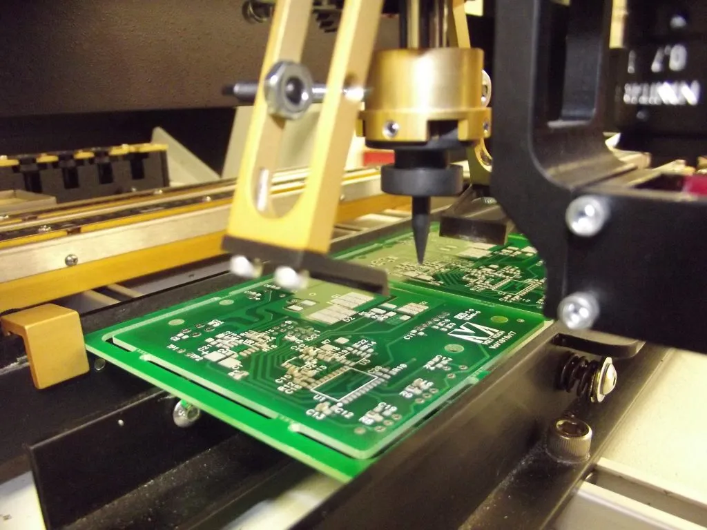
Mechanical carbide drills create precise holes, with parameters adjusted for laminate hardness. Post-drill, deburring removes burrs via chemical or plasma methods, ensuring smooth edges. Routing or milling finalizes NPTH slots if needed for irregular shapes.
Inspection verifies diameters and locations using automated optical systems. Solder mask application covers nearby areas but leaves NPTH open. Final fab steps like silkscreen and electrical test ignore NPTH conductivity.
This sequence reduces cycle time, as NPTH avoid panel plating and pattern plating cycles. Factory-driven processes per IPC-6012 yield high reliability for production runs.
NPTH Materials and Their Impact on Fabrication
NPTH fabrication uses the same core materials as general PCBs, primarily FR-4 laminates for rigidity and thermal stability. Hole walls expose epoxy resin and glass fibers, which must withstand mechanical insertion forces without fraying. High-Tg materials suit reflow environments where vent NPTH release trapped moisture.
Drill bits, typically tungsten carbide, endure repeated use on these materials. Aspect ratios guide material selection, as thicker stacks demand finer drills for NPTH. Surface finishes like HASL or ENIG on pads do not affect NPTH interiors.
Material consistency prevents drill bit wear, extending tool life in volume production. Engineers select dielectrics with low drill smear for cleaner NPTH post-desmear.
Factors Influencing NPTH Cost in PCB Production
NPTH cost advantages arise from eliminating plating chemicals, racks, and waste treatment associated with PTH. Drilling adds minimal expense, as shared equipment handles both hole types. Higher volumes amplify savings, with NPTH reducing overall fab time by 10-20% in mixed designs.
Tighter tolerances or small diameters increase costs due to specialized tooling. Board complexity, like layer count, indirectly affects NPTH via stackup stability. Fiducial NPTH add negligible cost but prevent assembly rework.
Procurement teams optimize by grouping NPTH in drill files, minimizing setups. Compared to PTH, NPTH lowers material use, appealing for budget-conscious projects.
NPTH Applications Across Industries
NPTH applications excel in mechanical fixation, such as screw holes for heat sinks or enclosures in power supplies. Fiducials enable precise SMT placement on panels. Vent holes mitigate popcorn effects during lead-free soldering by allowing vapor escape.
In automotive electronics, NPTH secure connectors against vibration. Tooling holes facilitate handling in automated lines. Landless NPTH save space in HDI boards for edge card guides.
These uses enhance reliability without electrical parasitics, suiting RF modules or sensors.
Best Practices and Troubleshooting for NPTH
Follow NPTH design guidelines by simulating fab tolerances early in layout. Specify NPTH separately in Gerber and drill files to prevent plating errors. Prototype testing confirms mechanical fit and thermal performance.
Common issues like burrs resolve with optimized feed rates. Misalignment traces to drill file errors; verify tooling holes first. For warpage, symmetric NPTH placement balances stress.
Adhere to J-STD-001 for assembly interfaces involving NPTH. Regular fab audits ensure consistency.
Conclusion
Non-plated through-hole technology offers electrical engineers a cost-effective, reliable solution for mechanical needs in PCB fabrication. Mastering NPTH design guidelines, manufacturing processes, and applications enables optimized boards with superior yield. By leveraging standard materials and processes, teams achieve robust designs compliant with IPC specifications. Integrating NPTH strategically reduces costs while enhancing functionality across diverse projects.
FAQs
Q1: What are the key NPTH design guidelines for high-reliability PCBs?
A1: NPTH design guidelines focus on minimum hole sizes, clearances from traces, and tolerances aligned with IPC-A-600 classes. Position fiducials away from edges for alignment accuracy. Symmetric placement prevents warpage, and separate drill files ensure no plating. These practices support dense layouts without compromising mechanical integrity.
Q2: How does the NPTH manufacturing process differ from PTH in PCB fabrication?
A2: The NPTH manufacturing process skips electroless copper and electrolytic plating after initial drilling. PTH holes are plated first, then NPTH drilled to avoid metallization. Deburring and inspection follow, integrating into standard flows for efficiency. This reduces steps and costs while maintaining precision.
Q3: What are common NPTH applications in electrical engineering projects?
A3: NPTH applications include mounting holes for screws and standoffs, vent holes for outgassing, and fiducials for assembly. They suit chassis integration, thermal management, and panelization without electrical connections. In RF designs, NPTH minimize signal disruption.
Q4: How does NPTH cost compare to PTH and impact overall PCB fabrication budgets?
A4: NPTH cost less due to no plating processes, saving on materials and handling. Factors like diameter and quantity influence pricing, but volume production amplifies benefits. Engineers balance NPTH use to cut fab expenses without design trade-offs.
References
IPC-6012E — Qualification and Performance Specification for Rigid Printed Boards. IPC, 2017
IPC-A-600K — Acceptability of Printed Boards. IPC, 2020
J-STD-001G — Requirements for Soldered Electrical and Electronic Assemblies. IPC, 2017


