Introduction
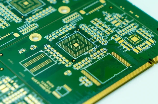
In the realm of printed circuit board (PCB) design and manufacturing, every detail impacts performance and reliability. One critical aspect often overlooked is the dry film solder mask thickness. This thin protective layer shields copper traces from oxidation, prevents solder bridging, and ensures electrical insulation. For electrical engineers, understanding dry film solder mask thickness requirements is vital for achieving optimal PCB performance, especially in high-density designs. This guide explores the technical principles behind solder mask thickness, its influence on PCB functionality, and adherence to industry standards like those from IPC. Whether designing for consumer electronics or aerospace applications, selecting the right thickness can make or break a project's success. Let's dive into the specifics of this essential PCB component.
What Is Dry Film Solder Mask and Why It Matters
A dry film solder mask is a polymer layer applied to a PCB to protect copper traces and define solderable areas. Unlike liquid photoimageable solder masks, dry film is a solid sheet laminated onto the board, then exposed and developed to create precise openings for soldering. This method offers uniform thickness and is often preferred for high-precision applications. The thickness of this layer directly affects insulation, durability, and manufacturability.
Why does it matter? Incorrect thickness can lead to issues like insufficient insulation, causing electrical shorts, or excessive coverage, hindering solderability. For high-density PCBs, where component spacing is tight, the balance is even more critical. Ensuring the right dry film solder mask thickness vs performance is a key factor in meeting design specifications and maintaining signal integrity. It also plays a role in thermal management and long-term reliability under varying environmental conditions.
Technical Principles of Dry Film Solder Mask Thickness
The thickness of a dry film solder mask typically ranges between 0.8 to 1.5 mils (20 to 38 micrometers), though specific applications may require adjustments. This range is influenced by factors such as the PCB's intended use, the density of components, and the manufacturing process. Let's break down the core principles affecting thickness selection.
Insulation and Dielectric Strength
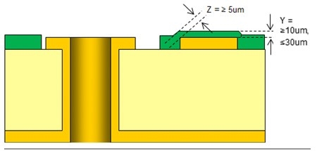
The primary role of a solder mask is to provide electrical insulation. Thicker layers enhance dielectric strength, preventing leakage currents between closely spaced traces. This is crucial for HDI PCBs where trace spacing can be as tight as a few mils. However, overly thick layers may cause issues during lamination, leading to uneven coverage or voids.
Solderability and Component Placement
Thickness also impacts solderability. A thinner solder mask allows for better solder wetting on pads, essential for surface-mount components. Conversely, a thicker mask might create a step height that interferes with component placement or solder paste application, risking defects like tombstoning.
Thermal and Mechanical Stress
PCBs experience thermal cycles during assembly and operation. A solder mask that is too thin may crack under stress, exposing copper to oxidation. A thicker mask offers better mechanical protection but could delaminate if not properly adhered. Balancing these factors ensures durability in harsh environments.
Manufacturing Constraints
Dry film application involves lamination under heat and pressure. Thickness must be compatible with equipment capabilities and board materials to avoid defects like bubbles or incomplete coverage. Standards such as IPC-SM-840E provide guidelines on acceptable thickness ranges and performance criteria for solder masks.

Suggested Reading: Mastering the Dry Film Solder Mask Exposure Process: A Step by Step Tutorial
Impact of Dry Film Solder Mask Thickness on PCB Performance
Understanding dry film solder mask thickness vs performance is essential for optimizing PCB designs. Here are the key areas where thickness influences functionality.
Signal Integrity in High-Density Designs
For high-density PCBs, trace spacing is minimal, often below 5 mils. A solder mask that is too thick can encroach on pads, reducing the effective solderable area and risking signal crosstalk. Conversely, a thin mask might not provide adequate insulation, leading to parasitic capacitance. Selecting the appropriate dry film solder mask thickness for high-density PCBs ensures both isolation and reliable connections.
Thermal Management
Solder mask thickness affects heat dissipation. A thicker layer can act as a thermal barrier, trapping heat in copper traces, which may degrade performance in power-intensive applications. A thinner mask allows better heat transfer but offers less protection against thermal shock. Engineers must consider operating temperatures when specifying thickness.
Environmental Resistance
PCBs in harsh environments, such as automotive or industrial settings, require robust protection. A thicker solder mask improves resistance to moisture, chemicals, and abrasion. However, if the layer is too thick, it may become brittle, cracking under vibration or thermal expansion. Standards like IPC-A-600K outline acceptability criteria for solder mask integrity under such conditions.
Practical Guidelines for Selecting Dry Film Solder Mask Thickness
Choosing the right dry film solder mask thickness requires balancing performance needs with manufacturing capabilities. Below are actionable steps for electrical engineers to follow.
Assess Design Requirements
Start by evaluating the PCB's application. High-frequency designs may need thinner masks to minimize dielectric effects, while power electronics might benefit from thicker layers for insulation. Define trace spacing, component types, and environmental factors to narrow down thickness options.
Refer to IPC Standards for Dry Film Solder Mask Thickness
Industry standards provide a reliable baseline. IPC-SM-840E, which governs solder mask performance, specifies qualification tests for adhesion, hardness, and thickness uniformity. While it does not mandate a specific thickness, it emphasizes that the mask must meet dielectric and coverage requirements for the intended class of PCB, whether Class 1, 2, or 3 as per IPC-6012E.
Collaborate with Manufacturing Teams
Work closely with fabrication partners to understand their process capabilities. Dry film thickness must align with lamination equipment and material properties. Request test samples to verify that the chosen thickness meets design goals without introducing defects like tenting over vias or incomplete coverage.
Test and Validate Thickness
Once a thickness is selected, validate it through prototyping. Measuring dry film solder mask thickness can be done using cross-sectional analysis or non-destructive methods like optical profilometry. Ensure the measured values fall within the specified range and check for performance under thermal cycling and humidity tests as per IPC-TM-650 test methods.
Best Practices for High-Density PCB Applications
High-density interconnect (HDI) designs present unique challenges for solder mask application. Here are targeted best practices for dry film solder mask thickness in such scenarios.
-
Opt for Thinner Layers: HDI boards often require masks below 1 mil to accommodate fine-pitch components. This ensures precise pad exposure without overlap.
-
Ensure Uniformity: Variations in thickness can cause uneven soldering. Use high-quality dry film materials and control lamination parameters for consistency.
-
Verify Via Tenting: For vias in HDI designs, the solder mask must fully tent openings to prevent solder wicking. Adjust thickness to balance tenting reliability with manufacturability.
-
Adhere to Standards: Follow IPC-6012E for HDI PCB performance specifications, ensuring the solder mask meets Class 3 requirements if designing for critical applications.
Common Challenges and Troubleshooting Tips
Even with careful planning, issues with dry film solder mask thickness can arise. Below are common problems and solutions.
Incomplete Coverage
If the mask fails to cover copper traces, it may be due to insufficient thickness or poor lamination. Increase the film thickness slightly or adjust pressure and temperature settings during application. Verify results against IPC-A-600K acceptability standards.
Solder Bridging
Excessive thickness near pads can cause solder to bridge during reflow. Reduce the mask thickness or refine the photolithography process to ensure precise openings. Test solderability using methods outlined in IPC-TM-650.
Delamination or Cracking
A mask that is too thick may delaminate under thermal stress. Select a thickness compatible with the board's coefficient of thermal expansion. Conduct adhesion tests as per IPC-SM-840E to confirm performance.
Conclusion
Selecting the right dry film solder mask thickness is a pivotal decision in PCB design and manufacturing. It influences insulation, solderability, and overall reliability, particularly for high-density PCBs. By understanding dry film solder mask thickness requirements and aligning with IPC standards for dry film solder mask thickness, engineers can optimize performance for diverse applications. Practical steps like assessing design needs, collaborating with manufacturers, and validating through testing ensure the chosen thickness meets both functional and environmental demands. With careful consideration, the solder mask becomes a robust shield, enhancing PCB longevity and efficiency in even the most challenging conditions.
FAQs
Q1: What are the dry film solder mask thickness requirements for consumer electronics PCBs?
A1: For consumer electronics, dry film solder mask thickness typically ranges from 0.8 to 1.2 mils to balance insulation and solderability. This range suits moderate trace densities and ensures compatibility with standard manufacturing processes. Always align with IPC-SM-840E for performance criteria, focusing on dielectric strength and adhesion to prevent failures in everyday use.
Q2: How does dry film solder mask thickness vs performance affect high-frequency PCB designs?
A2: In high-frequency PCBs, dry film solder mask thickness impacts signal integrity. A thinner mask, around 0.8 mils, minimizes dielectric interference and parasitic capacitance between traces. Thicker masks may degrade signal quality. Engineers must prioritize precise thickness control and validate performance through testing to maintain signal fidelity.
Q3: What methods are used for measuring dry film solder mask thickness accurately?
A3: Measuring dry film solder mask thickness can be done via cross-sectional microscopy for direct observation or optical profilometry for non-destructive analysis. Both methods provide precise measurements to ensure compliance with design specs. Refer to IPC-TM-650 for standardized test procedures to confirm uniformity and adherence to specified ranges.
Q4: How do IPC standards for dry film solder mask thickness guide high-density PCB manufacturing?
A4: IPC standards like IPC-SM-840E and IPC-6012E provide guidelines on solder mask performance for high-density PCBs. They outline requirements for insulation, adhesion, and coverage without mandating specific thickness values. These standards help engineers ensure the mask supports tight trace spacing and fine-pitch components in demanding applications.
References
IPC-SM-840E — Qualification and Performance of Permanent Solder Mask and Flexible Cover Materials. IPC, 2017.
IPC-6012E — Qualification and Performance Specification for Rigid Printed Boards. IPC, 2020.
IPC-A-600K — Acceptability of Printed Boards. IPC, 2020.
IPC-TM-650 — Test Methods Manual. IPC, Current Revision.


