Introduction
High-power electronics systems, including power supplies, inverters, and electric vehicle controllers, operate under intense electrical loads that generate substantial heat. Without proper thermal management, this heat can degrade components, compromise signal integrity, and shorten operational lifespan. Printed circuit boards form the foundation of these designs, and their material choices directly impact heat dissipation efficiency. 3 oz copper PCBs emerge as a key solution in high power PCB design, offering thicker conductive layers that enhance heat spreading. This article delves into the engineering principles behind their use, alongside critical features like 3 oz copper PCB thermal vias, PCB thermal pads, and PCB heat sinks. By understanding these elements, engineers can implement robust PCB cooling techniques for reliable performance.
What Are 3 oz Copper PCBs and Why Do They Matter?
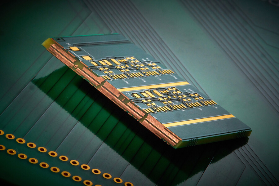
3 oz copper PCBs incorporate copper layers significantly thicker than the standard 1 oz found in general-purpose boards. This thickness upgrade boosts both electrical current-carrying capacity and thermal conductivity, making them ideal for applications where heat dissipation is paramount. In high-power scenarios, thinner copper leads to excessive resistive heating, while 3 oz layers distribute thermal loads more evenly across the board. Industry guidelines, such as those in IPC-2221, emphasize selecting appropriate copper weights to meet design requirements for thermal management.
The relevance stems from the growing demand in sectors like renewable energy and industrial automation, where power densities continue to rise. Thicker copper reduces the thermal resistance between heat sources and dissipation paths, preventing hotspots that could trigger failures. Engineers specify 3 oz copper to align with performance needs without relying solely on external cooling. This approach integrates seamlessly into multilayer stackups, supporting complex high power PCB designs.
Fundamental Thermal Challenges in High-Power Electronics
Heat in PCBs arises primarily from joule losses in conductors and switching inefficiencies in power semiconductors. These sources create localized hotspots that propagate through the board, stressing dielectrics and solder joints. Standard FR-4 substrates offer modest thermal conductivity, shifting reliance to copper planes for effective spreading. Inadequate management leads to issues like via cracking or laminate delamination under cyclic thermal stress.
Engineers must account for ambient conditions, enclosure airflow, and component derating to maintain junction temperatures within limits. High power PCB design demands a holistic view, balancing electrical, mechanical, and thermal domains. Ignoring these interactions risks non-compliance with reliability standards like J-STD-001 for soldered assemblies. Proactive thermal analysis from the schematic stage prevents costly redesigns.
Heat Transfer Principles in Thick Copper PCBs
Conduction dominates heat transfer in PCBs, governed by material properties and geometry. Copper's superior thermal conductivity enables rapid lateral spreading from components to board edges. 3 oz layers lower the effective thermal resistance compared to thinner foils, facilitating uniform temperature profiles. Vertical transfer relies on interconnections like thermal vias to access all layers.
Convection occurs at exposed surfaces, augmented by airflow or fins, while radiation contributes minimally at typical operating regimes. Multilayer boards leverage plane capacitance for shielding alongside thermal paths. Simulations reveal how copper thickness influences isotherms, guiding optimizations. These mechanisms underpin all PCB cooling techniques.
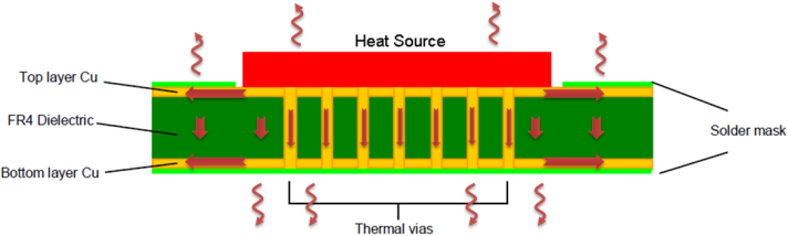
The Critical Role of 3 oz Copper PCB Thermal Vias
3 oz copper PCB thermal vias consist of arrays of electroplated through-holes positioned under heat-generating devices. They provide low-resistance conduits for heat to flow from top layers to buried planes or the opposite side. Dense via fields, often staggered for even distribution, maximize vertical conduction without compromising routing space. Filling vias with conductive materials further reduces voids and enhances reliability.
Design considerations include via diameter, pitch, and plating thickness to withstand thermal expansion mismatches. Tenting the solder mask over vias prevents contamination during assembly while maintaining paths open. In high power PCB design, these vias complement thick copper by bridging horizontal spreading with vertical escape routes. Qualification per IPC-6012 ensures they endure environmental stresses.
Proper simulation verifies via farm efficacy, adjusting density based on power dissipation profiles. This targeted approach avoids overdesign, preserving board real estate for signals.
Optimizing PCB Thermal Pads for Heat Spreading
PCB thermal pads are expansive copper pour areas aligned with component thermal interfaces. They capture heat directly from device bases, channeling it into the surrounding 3 oz copper plane. Integration with underlying thermal vias creates a composite path for dissipation. Mask clearance exposes pads for reliable solder wetting and sink attachment.
Layout rules dictate pad size relative to component footprint, avoiding sharp corners that concentrate stress. In multilayer configurations, pads connect multiple layers for compounded spreading. This feature proves essential in dense high power layouts where space constrains other solutions. Surface finishes like ENIG enhance pad durability under thermal cycling.
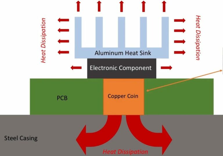
Integrating PCB Heat Sinks in Thick Copper Designs
PCB heat sinks mount to thermal pads via mechanical fasteners, adhesives, or clips, leveraging the conductivity of 3 oz copper planes. Fins increase surface area for convection, with orientation matching dominant airflow. Thermal interface materials bridge gaps, ensuring intimate contact without air pockets. Selection balances weight, cost, and thermal resistance for the application.
In forced-air systems, sinks pair with fans for active cooling, scaling to power levels. Board stiffening prevents warpage under sink torque. This passive-to-active spectrum fits varied enclosure constraints. Combined with vias and pads, sinks form a tiered PCB cooling technique hierarchy.
Comprehensive PCB Cooling Techniques for High-Power Applications
High power PCB design employs layered strategies: intrinsic copper spreading, vias for depth, pads for capture, and sinks for rejection. Active methods like thermoelectric coolers suit extreme cases, while passive relies on geometry. Hybrid stackups with dedicated thermal layers optimize paths. Maintenance factors, such as dust filters, sustain long-term efficacy.
Per IPC-2152, conductor sizing ties directly to allowable temperature rises, informing copper weight choices. Iterative prototyping validates models against real loads. Documentation of thermal margins aids scalability.
Best Practices and Troubleshooting Insights
Begin with stackup planning, allocating 3 oz to power layers while reserving thinner for signals. Simulate hotspot migrations, refining via and pad geometries. Prototype testing under accelerated conditions reveals weaknesses like via plug failures. DFM collaboration ensures thick copper etch uniformity.
Troubleshoot hotspots via infrared imaging, correlating to design elements. Adjust airflow or add secondary sinks as needed. Standardize libraries for repeatable thermal primitives. These practices yield robust, manufacturable designs.
Conclusion
3 oz copper PCBs anchor thermal management in high-power electronics by amplifying conduction alongside 3 oz copper PCB thermal vias, PCB thermal pads, PCB heat sinks, and broader PCB cooling techniques. This synergy addresses heat challenges logically, enhancing reliability per industry benchmarks. Engineers gain actionable tools for high power PCB design, from principles to implementation.
As power demands evolve, thicker copper remains a cornerstone, adaptable to emerging needs. Prioritizing these elements ensures systems perform under stress, minimizing failures.
FAQs
Q1: What advantages do 3 oz copper PCB thermal vias offer in high power designs?
A1: 3 oz copper PCB thermal vias enable efficient vertical heat transfer from surface components to inner layers, reducing hotspot severity. Arrays under devices distribute loads evenly, leveraging thick copper spreading. Filling options cut resistance further. This aligns with standards for thermal reliability in demanding applications.
Q2: How do PCB thermal pads integrate with PCB heat sinks?
A2: PCB thermal pads provide direct copper interfaces for PCB heat sinks, minimizing contact resistance via interface materials. Paired with thermal vias, they channel heat effectively in 3 oz copper boards. Proper exposure and coplanarity ensure optimal performance. Essential for PCB cooling techniques in high-power setups.
Q3: Why prioritize PCB cooling techniques in high power PCB design?
A3: PCB cooling techniques like vias, pads, and sinks prevent thermal runaway, preserving component life and efficiency. Thick copper enhances conduction, but integrated features handle peak loads. Simulations and testing validate choices. Critical for compliance and field reliability.
Q4: When should engineers select 3 oz copper for thermal management?
A4: Select 3 oz copper when standard thicknesses yield excessive temperature rises per current needs. It supports high power PCB design with better dissipation and current capacity. Combine with thermal vias for superior results. Factory processes maintain integrity.
References
IPC-2221 — Generic Standard on Printed Board Design. IPC
IPC-2152 — Standard for Determining Current-Carrying Capacity in Printed Boards. IPC
IPC-6012 — Qualification and Performance Specification for Rigid Printed Boards. IPC
J-STD-001 — Requirements for Soldered Electrical and Electronic Assemblies. IPC


