Introduction
In the realm of modern electronics, high speed design has become a cornerstone for applications requiring rapid data transmission and minimal signal delays. Thick PCB materials play a pivotal role in supporting these demanding requirements, offering structural integrity and enhanced performance for complex circuits. As data rates climb into the multi-gigabit range, selecting the right materials for thick PCBs is crucial to manage signal losses and ensure reliability. This article explores the significance of thick PCBs in high speed applications, delving into material considerations, stack up plans, and strategies to mitigate signal degradation. Aimed at electrical engineers, the content provides a detailed understanding of how thick PCB construction influences performance in cutting edge technologies like 5G, IoT, and advanced computing systems.
What Are Thick PCBs and Why Do They Matter
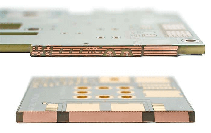
Thick PCBs are defined as printed circuit boards with a total thickness exceeding standard dimensions, often greater than 2.0 mm, to accommodate multiple layers or enhanced durability. In high speed design, these boards are essential for supporting intricate stack up plans that integrate numerous signal and power layers. Their increased thickness provides mechanical stability, crucial for large form factor devices or those subjected to harsh environments. Moreover, thick PCBs can handle higher current capacities and offer better thermal dissipation, both vital for high speed applications where heat generation is a concern. Their relevance lies in enabling reliable performance for systems requiring consistent signal integrity over long distances or at elevated frequencies, ensuring that data intensive applications function without compromise.
Technical Principles of Thick PCBs in High Speed Design
High speed design focuses on maintaining signal integrity at elevated frequencies, typically above 1 GHz, where signal losses become pronounced. Thick PCBs influence this through several technical aspects. First, the dielectric properties of the substrate material affect the propagation speed and attenuation of signals. Materials with low dielectric constants and low loss tangents are preferred to minimize delays and energy dissipation. Second, the increased thickness often correlates with more layers in the stack up plan, which can introduce complexities in impedance control. Mismatched impedance between layers leads to reflections, degrading signal quality.
Additionally, conductor losses arise from the skin effect, where high frequency signals travel primarily on the surface of traces, increasing resistance. Dielectric losses also contribute, as the substrate absorbs signal energy, particularly in thicker boards with longer signal paths. Crosstalk, another concern, worsens in dense layouts common to thick PCBs, as adjacent traces interfere with each other. Addressing these challenges requires precise design and material selection aligned with standards like IPC-6012E, which outlines performance specifications for rigid boards.
Material Considerations for Thick PCBs in High Speed Applications
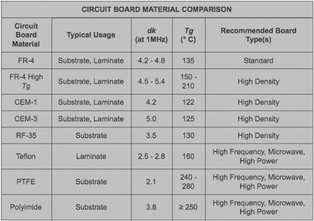
Selecting materials for thick PCBs in high speed applications involves balancing electrical performance with manufacturability. Substrates with low dielectric constants, often below 3.5, reduce signal propagation delays, while low loss tangents minimize energy absorption. These properties are critical for maintaining signal integrity over extended trace lengths typical in thicker boards. Thermal stability is another factor, as high speed circuits generate significant heat, requiring materials that resist degradation under elevated temperatures.
Copper foil type also impacts performance. Smoother copper surfaces reduce conductor losses at high frequencies by limiting the skin effect. The choice of copper weight, often heavier in thick PCBs, supports higher current demands but must be optimized to avoid excessive signal attenuation. Adherence to standards such as IPC-4562, which specifies copper foil requirements, ensures consistent quality. Engineers must also consider the glass transition temperature of materials to prevent warping during thermal cycles, a common issue in thick PCB construction.
Related Reading: HDI PCB Materials Selection for High Frequency Applications
Stack Up Plan for Thick PCBs in High Speed Design
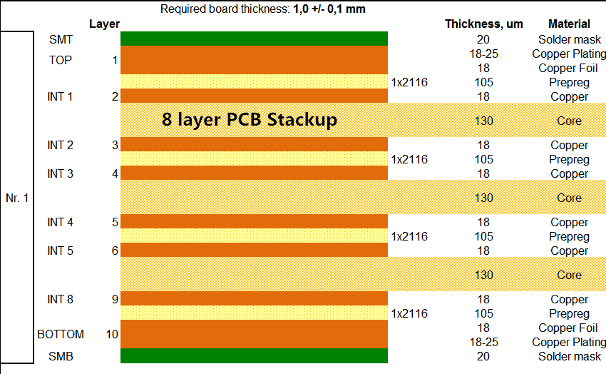
A well designed stack up plan is fundamental to thick PCBs used in high speed applications. The arrangement of signal, ground, and power layers directly influences impedance control and signal isolation. Typically, thick PCBs feature eight or more layers, necessitating careful planning to minimize crosstalk and maintain consistent dielectric spacing. Ground planes should be placed adjacent to signal layers to provide a stable reference and reduce electromagnetic interference.
Symmetry in the stack up is vital to prevent mechanical stress and warping, especially in thicker boards. Alternating signal and plane layers help achieve this balance while ensuring uniform impedance across the board. Controlled dielectric thickness between layers, as specified in standards like IPC-4101, aids in meeting target impedance values. Engineers often use simulation tools to validate the stack up design before fabrication, ensuring signal integrity is preserved across all high speed traces.
Signal Losses in Thick PCBs and Mitigation Strategies
Signal losses in thick PCBs for high speed applications stem from multiple sources, including dielectric absorption, conductor resistance, and crosstalk. Dielectric losses occur when the substrate material absorbs signal energy, a problem exacerbated by thicker boards with greater material volume. Conductor losses increase due to the skin effect at high frequencies, where current concentrates on trace surfaces, raising effective resistance. Crosstalk arises from electromagnetic coupling between closely spaced traces, a frequent issue in dense, multilayer designs.
Mitigation begins with material selection, prioritizing substrates with low loss characteristics. Trace geometry also plays a role, where wider traces reduce resistance but may increase capacitance, necessitating a balance. Implementing ground planes between signal layers shields traces from interference, while maintaining consistent spacing controls impedance. Adhering to test methods outlined in IPC-TM-650 ensures accurate measurement of signal performance during design validation. Additionally, minimizing via usage in high speed paths reduces discontinuities that contribute to signal degradation.
Related Reading: Beyond FR-4: Exploring Advanced PCB Materials for High-Frequency Applications
Practical Solutions for Optimizing Thick PCBs in High Speed Design
Designing thick PCBs for high speed applications demands actionable strategies to ensure performance. Start with a robust stack up plan that prioritizes symmetry and impedance control, using ground planes to isolate signal layers. Select materials with verified low loss properties, referencing standards like IPC-4101 for dielectric specifications. Optimize trace routing by avoiding sharp bends and maintaining uniform widths to prevent reflections.
Thermal management is equally important. Incorporate thermal vias or thicker copper layers to dissipate heat effectively, protecting signal integrity under load. Validate designs through simulation to predict signal behavior across frequencies, adjusting parameters as needed before fabrication. During manufacturing, ensure compliance with IPC-6012E for quality and performance consistency. Finally, test prototypes under real world conditions to identify potential signal losses or interference, refining the design iteratively for optimal results.
Conclusion
Thick PCB materials are indispensable for high speed applications, providing the structural and electrical foundation for cutting edge technologies. Their role in supporting complex stack up plans and managing signal losses cannot be overstated. By understanding the technical principles behind signal integrity and applying practical solutions like optimized material selection and precise stack up design, engineers can overcome the challenges inherent in thick PCB construction. Adherence to established industry standards ensures reliability and performance, enabling seamless data transmission in demanding environments. As high speed design continues to evolve, mastering the use of thick PCBs will remain a critical skill for advancing electronic innovation.
FAQs
Q1: What are the key benefits of using thick PCBs in high speed design?
A2: Thick PCBs offer enhanced mechanical stability and support for multilayer stack up plans in high speed design. They handle higher currents and provide better thermal dissipation, crucial for maintaining signal integrity at elevated frequencies. Their thickness accommodates complex routing, reducing signal losses when paired with low loss materials, ensuring reliable performance in data intensive applications.
Q2: How do thick PCBs impact signal losses in high speed applications?
A2: Thick PCBs can increase signal losses due to greater dielectric material volume, leading to higher absorption. Conductor losses also rise from the skin effect at high frequencies. Proper material selection with low loss properties and optimized trace design, along with strategic stack up plans, help mitigate these losses effectively for high speed circuits.
Q3: What should a stack up plan consider for thick PCBs in high speed design?
A3: A stack up plan for thick PCBs must focus on symmetry to prevent warping and ensure impedance control. Ground planes should separate signal layers to reduce crosstalk. Consistent dielectric spacing, as per industry standards, maintains signal integrity. Balancing layer functions optimizes performance in high speed applications with multiple layers.
Q4: How can engineers reduce signal losses in thick PCB designs?
A4: Engineers can reduce signal losses in thick PCB designs by choosing low loss dielectric materials and smoother copper foils. Implementing ground planes, optimizing trace geometry, and minimizing vias help maintain signal quality. Validating designs through simulation and adhering to test standards ensures minimal degradation in high speed applications.
References
IPC-6012E — Qualification and Performance Specification for Rigid Printed Boards. IPC, 2020.
IPC-4101E — Specification for Base Materials for Rigid and Multilayer Printed Boards. IPC, 2021.
IPC-4562A — Metal Foil for Printed Board Applications. IPC, 2008.
IPC-TM-650 — Test Methods Manual. IPC, Current Edition.


