Introduction
High-Density Interconnect (HDI) Printed Circuit Boards (PCBs) are critical in modern electronics, enabling compact designs with high performance in devices like smartphones, medical equipment, and automotive systems. These boards feature fine lines, small vias, and dense component placement, which make them susceptible to unique manufacturing and operational challenges. For electrical engineers, understanding how to troubleshoot common HDI PCB problems is essential to ensure reliability and functionality. This guide offers a detailed HDI PCB troubleshooting guide, focusing on failure analysis and common defects. It aims to equip engineers with practical strategies to identify, analyze, and resolve issues in HDI PCB designs and assemblies. By addressing these challenges systematically, professionals can minimize downtime, reduce costs, and maintain product quality in demanding applications.
What Are HDI PCBs and Why Do They Matter?
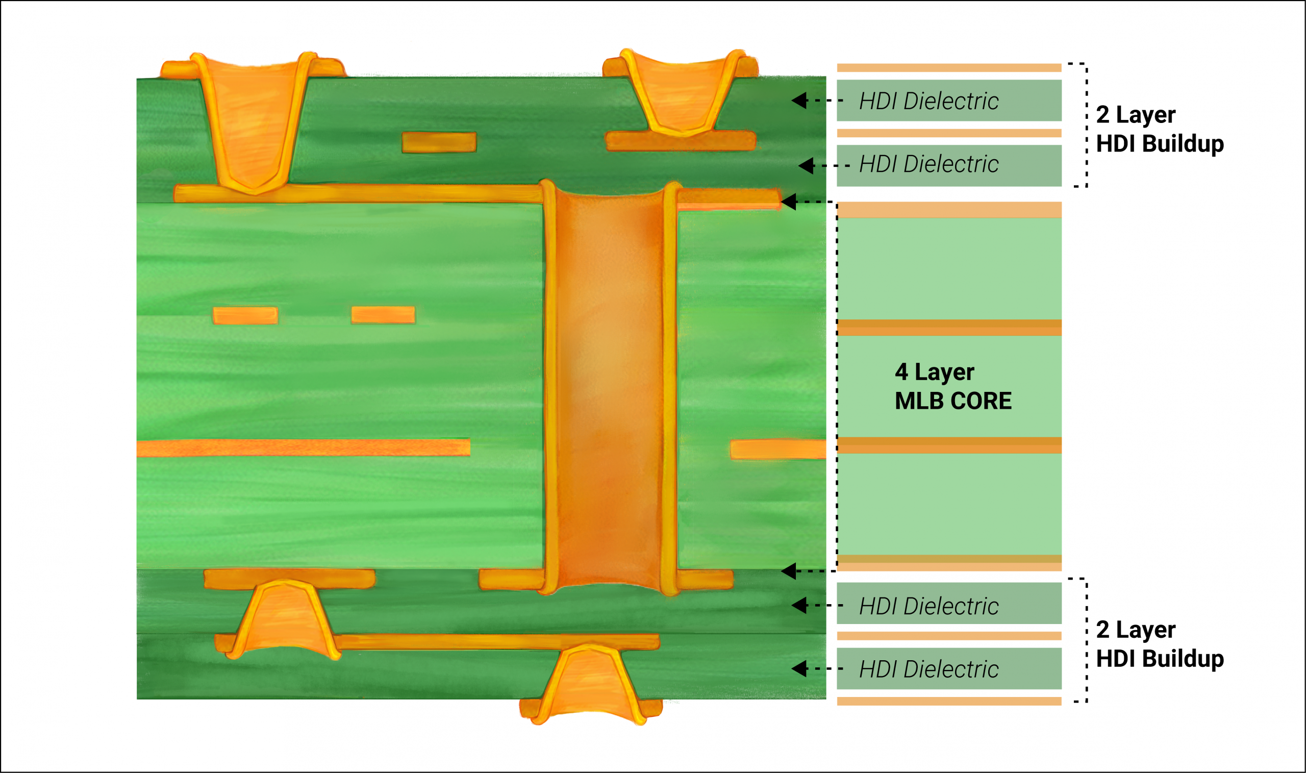
HDI PCBs are advanced circuit boards designed to accommodate a higher density of components in a smaller footprint. They utilize microvias, blind vias, buried vias, and finer trace widths to achieve complex routing in multilayer structures. These characteristics make HDI PCBs ideal for high-speed, high-performance applications where space and signal integrity are critical. However, the complexity of HDI designs introduces specific risks, such as signal interference, manufacturing defects, and thermal stress failures. For electrical engineers, mastering HDI PCB failure analysis is vital to prevent costly redesigns and ensure compliance with industry standards. The ability to identify and resolve common HDI PCB defects directly impacts product reliability and time to market, making troubleshooting skills a cornerstone of effective PCB engineering.
Technical Causes of HDI PCB Failures
Understanding the root causes of HDI PCB failures requires a deep dive into design, manufacturing, and operational factors. Below are key technical issues that frequently affect HDI boards.
Microvia Failures
Microvias, with diameters often below 150 micrometers, are prone to defects due to their small size and the precision required in drilling and plating. Common issues include incomplete copper plating, leading to open circuits, or cracks caused by thermal expansion during operation. These failures often result from improper aspect ratio control or inadequate material selection for thermal stability.
Related Reading: Troubleshooting Microvia PCB Defects: A Guide to Identifying and Resolving Common Issues
Signal Integrity Problems
HDI PCBs often operate at high frequencies, making signal integrity a critical concern. Crosstalk, impedance mismatches, and electromagnetic interference can degrade performance. These issues typically stem from insufficient spacing between traces, improper stack-up design, or lack of ground plane shielding. Maintaining controlled impedance is essential to prevent signal distortion in dense layouts.
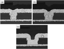
Delamination and Warpage
Delamination occurs when layers of the PCB separate due to poor adhesion or moisture ingress, often exacerbated by thermal cycling. Warpage, on the other hand, results from uneven thermal expansion or mechanical stress during manufacturing. Both defects compromise structural integrity and can lead to component misalignment or solder joint failures in HDI designs.
Related Reading: Minimizing Warpage in Multilayer PCB Manufacturing: Causes and Cures
Solder Joint Defects
In HDI assemblies, solder joint reliability is challenged by fine-pitch components and smaller pads. Common defects include insufficient solder volume, voids, or cracks due to thermal fatigue. These issues often arise from incorrect reflow profiles or contamination on the board surface, impacting electrical connectivity.
Common HDI PCB Defects and Identification Methods
Identifying common HDI PCB defects early is crucial for effective troubleshooting. Here are the most frequent issues and methods to detect them, tailored for electrical engineers.
Visual and Microscopic Inspection
Visual inspection under magnification can reveal surface defects like scratches, misaligned layers, or visible cracks in microvias. Advanced tools such as optical microscopes or scanning electron microscopy provide deeper insights into subsurface issues, particularly for detecting plating voids or delamination.
Electrical Testing for Continuity and Shorts
Electrical testing using multimeters or automated test equipment helps identify open circuits, shorts, or resistance anomalies in HDI PCBs. Techniques like Time-Domain Reflectometry (TDR) are particularly useful for pinpointing impedance discontinuities in high-speed signal paths, aiding in HDI PCB failure analysis.
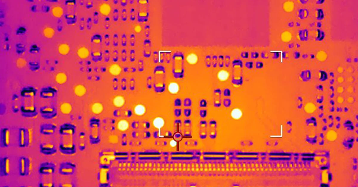
Thermal Imaging for Hotspots
Thermal imaging cameras detect overheating areas on the board, often indicating high-resistance connections or failing components. This non-destructive method is effective for identifying solder joint issues or power distribution problems in densely packed HDI layouts during operation.
X-Ray Inspection for Hidden Defects
X-ray imaging is invaluable for inspecting internal structures of HDI PCBs, such as buried vias or inner layer alignments. It can uncover voids in solder joints, misregistrations, or cracks not visible through surface inspection, ensuring thorough defect identification.
Practical Solutions for HDI PCB Troubleshooting
Addressing HDI PCB issues requires a systematic approach grounded in industry best practices. Below are actionable solutions for common problems, designed to assist electrical engineers in maintaining board reliability.
Optimizing Design for Manufacturability
Ensure that HDI PCB designs adhere to manufacturability guidelines by maintaining appropriate aspect ratios for microvias, typically as specified in standards like IPC-2226. Incorporate adequate spacing between traces to minimize crosstalk and verify stack-up configurations for signal integrity. Simulation tools can predict potential issues before fabrication begins.
Enhancing Manufacturing Process Controls
During manufacturing, strict adherence to material selection and process parameters is critical. Use materials with low coefficients of thermal expansion to reduce warpage risks. Implement precise laser drilling for microvias and ensure consistent copper plating thickness to avoid connectivity failures, aligning with standards such as IPC-6012E.
Improving Assembly Techniques
For assembly, optimize reflow soldering profiles to match the thermal characteristics of HDI components. Cleanliness of the board surface must be maintained to prevent contamination-related solder defects. Employ automated optical inspection systems post-assembly to catch misalignments or insufficient solder early in the process.
Implementing Robust Testing Protocols
Adopt comprehensive testing protocols that include in-circuit testing and functional testing to validate HDI PCB performance. Use environmental stress testing, such as thermal cycling per IPC-TM-650, to simulate operational conditions and uncover latent defects like delamination or microvia cracks before deployment.
Advanced Troubleshooting Insights for HDI PCBs
For complex HDI PCB issues, advanced techniques can provide deeper insights. Failure analysis often involves cross-sectioning failed boards to examine microvia integrity or layer bonding under high magnification. Techniques like dye and pry testing can reveal hidden cracks in solder joints. Additionally, engineers should document recurring defects to identify patterns, which may point to systemic design or process flaws. Collaboration with material scientists can help in selecting substrates that better withstand thermal and mechanical stresses, especially in high-reliability applications. Referencing standards such as IPC-A-600K for acceptability criteria ensures that troubleshooting outcomes meet industry expectations for quality and performance.
Conclusion
Troubleshooting common HDI PCB problems demands a blend of technical knowledge, systematic analysis, and adherence to established standards. By understanding the causes of failures such as microvia defects, signal integrity issues, and delamination, electrical engineers can implement effective solutions to enhance board reliability. This HDI PCB troubleshooting guide emphasizes the importance of thorough inspection, precise manufacturing controls, and robust testing to address common HDI PCB defects. With a focus on practical strategies and failure analysis, engineers can mitigate risks, ensuring that HDI PCBs perform optimally in high-stakes applications. Staying aligned with industry standards further guarantees consistent quality and long-term success in complex electronic designs.
FAQs
Q1: What are the most common HDI PCB defects encountered in high-speed designs?
A1: In high-speed HDI PCB designs, common defects include microvia failures due to poor plating, signal integrity issues like crosstalk, and solder joint cracks from thermal stress. These problems often arise from dense layouts and fine geometries. Visual inspection, electrical testing, and X-ray analysis can help identify these issues early, ensuring reliability in critical applications.
Q2: How can HDI PCB failure analysis improve design reliability?
A2: HDI PCB failure analysis identifies root causes of defects, such as improper material selection or manufacturing errors, allowing engineers to refine designs. By analyzing failure patterns through techniques like thermal imaging and cross-sectioning, design rules can be adjusted to prevent recurrence. This process enhances long-term reliability and performance in demanding environments.
Q3: What standards should guide an HDI PCB troubleshooting guide?
A3: Standards like IPC-6012E for performance specifications and IPC-A-600K for acceptability criteria are essential for an HDI PCB troubleshooting guide. These provide benchmarks for quality, design, and manufacturing processes. Adhering to such guidelines ensures consistent troubleshooting outcomes and compliance with industry expectations for high-density interconnect boards.
Q4: How do I detect signal integrity issues in HDI PCBs during troubleshooting?
A4: Signal integrity issues in HDI PCBs can be detected using tools like oscilloscopes for waveform analysis and Time-Domain Reflectometry for impedance mismatches. Check for crosstalk or noise in high-speed traces. Ensuring proper grounding and trace spacing, as per design standards, helps resolve these common HDI PCB defects effectively during troubleshooting.
References
IPC-6012E — Qualification and Performance Specification for Rigid Printed Boards. IPC, 2020.
IPC-A-600K — Acceptability of Printed Boards. IPC, 2020.
IPC-2226 — Sectional Design Standard for High Density Interconnect (HDI) Printed Boards. IPC, 2003.
IPC-TM-650 — Test Methods Manual. IPC, 2021.


