Introduction
Double-layer PCBs are fundamental components in modern electronics, offering a balance of complexity and cost-effectiveness for a wide range of applications. These boards, with conductive layers on both sides of an insulating substrate, are widely used in consumer electronics, industrial controls, and automotive systems. However, their design and manufacturing intricacies often lead to issues that can compromise performance. For electrical engineers, mastering double-layer PCB troubleshooting is essential to ensure reliability and functionality. This guide provides a detailed approach to identifying and resolving common faults, focusing on practical PCB fault finding and testing methods. Whether you are debugging a prototype or addressing production failures, this PCB repair guide offers actionable insights to streamline the process and maintain high-quality standards in your projects.
What Are Double-Layer PCBs and Why Do They Matter
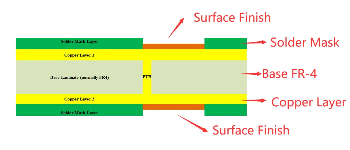
Double-layer PCBs, also known as two-layer boards, consist of two conductive copper layers separated by a dielectric material, typically PCB FR-4. Vias connect the layers, enabling complex routing in a compact form factor. These boards are a step up from single-layer designs, supporting more intricate circuits while remaining more affordable than multi-layer alternatives. Their importance lies in their versatility, making them ideal for devices like power supplies, LED lighting, and communication equipment.
For electrical engineers, understanding double-layer PCBs is critical because they often serve as the backbone of mid-range electronic products. Issues in these boards can lead to signal degradation, power failures, or complete system breakdowns. Effective PCB troubleshooting ensures that designs meet performance expectations and adhere to industry standards, reducing downtime and costly rework. With the right PCB testing techniques, engineers can pinpoint faults early and maintain project timelines.
Common Issues in Double-Layer PCBs
Double-layer PCBs, while robust, are prone to specific issues due to their structure and manufacturing processes. Identifying these problems is the first step in effective troubleshooting. Below are the most frequent challenges encountered.
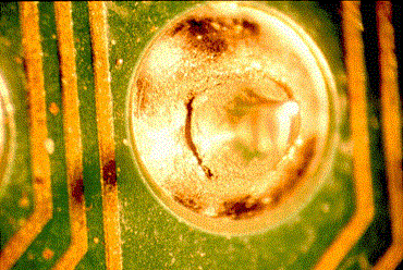
Solder Joint Failures
Solder joint issues often arise from thermal stress, improper soldering techniques, or contamination. Cracked or cold joints can interrupt connectivity between components and the board, leading to intermittent failures.
Delamination and Warpage
Delamination occurs when layers of the PCB separate, often due to moisture absorption or thermal expansion mismatches. Warpage, similarly, results from uneven heating or mechanical stress, affecting component alignment and soldering quality.
Signal Integrity Problems
With two conductive layers, signal crosstalk and electromagnetic interference become concerns, especially in high-speed designs. Poor grounding or improper trace spacing can degrade performance.
Via Failures
Vias are critical for interlayer connections, but defects like incomplete plating or cracks can disrupt conductivity. These issues often stem from manufacturing flaws or mechanical stress during assembly.
Suggested Reading: Via Strategies for High Density Double Layer PCBs: Types and Placement
Component Misplacement or Damage
Incorrectly placed or damaged components can cause short circuits or open connections. This is often a result of manual errors or inadequate inspection during assembly.
Technical Causes Behind Double-Layer PCB Failures
Understanding the root causes of failures is vital for effective double-layer PCB troubleshooting. Several factors contribute to these issues, often tied to design, manufacturing, or environmental conditions.
Design Errors
Inadequate trace width or spacing can lead to overheating or crosstalk. Failing to account for thermal dissipation in high-power circuits often results in component stress. Additionally, improper via placement can weaken the board structure, as outlined in standards like IPC-6012E, which specifies design and performance criteria for rigid printed boards.
Manufacturing Defects
During fabrication, issues like uneven copper plating or poor etching can create weak points in the board. Delamination often results from improper lamination processes or material inconsistencies, violating guidelines in IPC-A-600K for board acceptability. Contaminated surfaces may also prevent proper soldering, leading to joint failures.
Environmental Stress
Exposure to humidity, temperature fluctuations, or mechanical vibration can degrade PCB performance. Moisture ingress, for instance, can cause corrosion or delamination, while thermal cycling may crack solder joints. Standards like JEDEC J-STD-020E provide classifications for moisture sensitivity, guiding engineers on handling and storage.
Assembly Mishandling
Incorrect soldering temperatures or excessive force during component placement can damage the board or components. Overheating, in particular, risks desoldering adjacent parts or burning traces, emphasizing the need for controlled processes.
Practical Solutions for Double-Layer PCB Troubleshooting
Addressing issues in double-layer PCBs requires a systematic approach to PCB fault finding and repair. Below are actionable steps and best practices tailored for electrical engineers.
Step 1: Visual Inspection
Begin with a thorough visual check under adequate lighting or magnification. Look for obvious signs of damage, such as burnt components, cracked traces, or delaminated areas. Discoloration often indicates overheating, while bulging capacitors suggest electrical stress. This initial step aligns with IPC-A-600K guidelines for identifying surface defects.
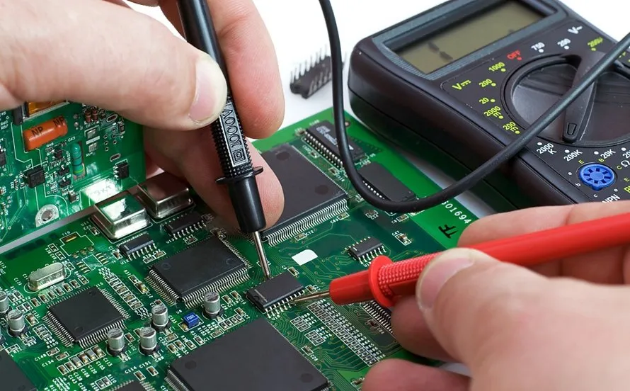
Step 2: Continuity and Resistance Testing
Use a multimeter to test for continuity between points on the board. Open circuits indicate broken traces or failed vias, while unexpected low resistance may signal a short. Focus on critical paths and compare readings against the schematic to isolate faults. This method is a cornerstone of PCB testing for verifying electrical integrity.
Step 3: Power-Up Testing with Caution
Apply power to the board in a controlled manner, using a current-limited power supply if possible. Monitor for abnormal behavior like excessive heat or voltage drops. Start with low voltage to minimize damage if a short exists. This approach helps in live PCB fault finding without risking further harm.
Step 4: Thermal Imaging for Hotspots
Thermal cameras can detect overheating components or traces, often pointing to high-resistance connections or failing parts. Focus on areas near power components, as they are prone to thermal issues. This technique enhances double-layer PCB troubleshooting by revealing hidden problems.
Step 5: Signal Analysis for Integrity Issues
For high-speed circuits, use an oscilloscope to check signal quality. Look for noise, crosstalk, or unexpected delays, which often stem from poor grounding or trace layout. Adjusting grounding planes or adding shielding may resolve these issues, ensuring reliable operation.
Step 6: Repair Techniques
Once faults are identified, apply targeted repairs. For broken traces, use conductive epoxy or jumper wires to restore connectivity. Replace damaged components with equivalents matching the original specifications. For delamination, localized repairs may suffice, though severe cases might require board replacement. Always document repairs for traceability.
Best Practices to Prevent Double-Layer PCB Issues
- Adhere to Design Standards: Follow guidelines in IPC-6012E for trace spacing, via sizing, and thermal management to minimize design-related failures.
- Select Quality Materials: Use substrates and components rated for the intended environment, referencing JEDEC J-STD-020E for moisture sensitivity levels.
- Control Assembly Conditions: Maintain consistent soldering temperatures and clean workspaces to avoid contamination or thermal damage.
- Perform Pre-Assembly Testing: Inspect bare boards for manufacturing defects before assembly, aligning with IPC-A-600K acceptability criteria.
- Implement Stress Testing: Simulate operating conditions to identify weak points early, using thermal cycling or vibration tests as needed.
Troubleshooting Case Insight: Resolving a Power Supply Failure
Consider a scenario where a double-layer PCB in a power supply unit fails to deliver stable output. Initial visual inspection reveals no obvious damage, but power-up testing shows erratic voltage. Using a multimeter, an engineer identifies a high-resistance connection near a via. Thermal imaging confirms a hotspot at the same location, suggesting a plating defect. By drilling out the faulty via and installing a jumper wire, connectivity is restored. Signal analysis post-repair ensures no interference, and the board passes final testing. This case underscores the importance of combining multiple PCB testing methods for accurate diagnosis and effective repair.
Conclusion
Double-layer PCBs are indispensable in electronics, but their complexity introduces challenges that demand skilled troubleshooting. By understanding common issues like solder joint failures, delamination, and signal integrity problems, electrical engineers can address faults efficiently. Systematic approaches, including visual inspection, continuity testing, and thermal imaging, form the backbone of double-layer PCB troubleshooting. Adhering to industry standards and best practices further minimizes risks, ensuring reliable performance. With the insights from this PCB repair guide, engineers are equipped to tackle faults confidently, maintaining quality and functionality in their designs.
FAQs
Q1: What are the most common causes of double-layer PCB failures during troubleshooting?
A1: Double-layer PCB troubleshooting often reveals failures from design errors, manufacturing defects, and environmental stress. Issues like improper trace spacing, poor soldering, or moisture exposure can disrupt performance. Thermal stress frequently cracks solder joints, while via defects interrupt connectivity. Following standards like IPC-6012E helps identify and mitigate these causes early.
Q2: How can I perform effective PCB fault finding on a double-layer board?
A2: For effective PCB fault finding, start with a visual inspection for physical damage. Use a multimeter to check continuity and resistance, identifying opens or shorts. Apply power cautiously to observe behavior, and use thermal imaging for hotspots. Combine these steps with schematic reference to isolate faults accurately.
Q3: What tools are essential for PCB testing in double-layer designs?
A3: Essential tools for PCB testing include a multimeter for continuity checks, an oscilloscope for signal analysis, and a thermal camera for detecting heat issues. A magnifying glass aids visual inspection, while a current-limited power supply ensures safe power-up testing. These tools collectively enable thorough diagnosis of double-layer boards.
Q4: How can I prevent signal integrity issues during double-layer PCB troubleshooting?
A4: Prevent signal integrity issues by ensuring proper grounding and trace spacing during design, adhering to standards like IPC-6012E. During double-layer PCB troubleshooting, use an oscilloscope to monitor noise or crosstalk. Adding shielding or adjusting layouts can resolve problems, maintaining reliable signal transmission in high-speed circuits.
References
IPC-6012E — Qualification and Performance Specification for Rigid Printed Boards. IPC, 2020.
IPC-A-600K — Acceptability of Printed Boards. IPC, 2020.
JEDEC J-STD-020E — Moisture/Reflow Sensitivity Classification for Nonhermetic Surface Mount Devices. JEDEC, 2014.


