Introduction
Creating multi-layer printed circuit boards (PCBs) at home is a rewarding yet challenging endeavor for electronic hobbyists. Home-etched multi-layer PCBs allow for compact designs and complex circuits, but they often come with unique issues that can frustrate even seasoned DIY enthusiasts. From misalignment of layers to etching inconsistencies, troubleshooting these problems requires patience and a systematic approach. This article explores common PCB etching problems in home-etched multi-layer designs, offers practical DIY PCB repair techniques, and provides actionable steps for multi-layer PCB troubleshooting. Whether you are a beginner or an experienced hobbyist, understanding these challenges and solutions will improve your home electronics repair skills and project outcomes. Let’s dive into the intricacies of multi-layer PCB fabrication and how to address issues effectively.
What Are Home-Etched Multi-Layer PCBs and Why Do They Matter?
Multilayer PCBs consist of multiple conductive layers separated by insulating material, stacked and bonded together. Unlike single or double-layer boards, they support intricate circuits in a smaller footprint, making them ideal for advanced electronic projects. For hobbyists, home-etching these boards offers a cost-effective way to prototype complex designs without relying on professional services.
However, the process introduces risks like layer misalignment, poor etching quality, and via connection failures. Addressing these issues is crucial because even minor defects can render a board unusable, wasting time and resources. Mastering multi-layer PCB troubleshooting not only saves projects but also builds valuable skills in home electronics repair. This knowledge empowers hobbyists to push the boundaries of DIY electronics with confidence.
Technical Causes of Issues in Home-Etched Multi-Layer PCBs
Understanding the root causes of PCB etching problems is the first step in effective troubleshooting. Multi-layer boards are more prone to errors due to their complexity. Below are key technical issues that hobbyists often encounter during the home-etching process.
Layer Misalignment During Stacking
One frequent problem is misalignment between layers when stacking them before bonding. Even a slight offset can disrupt via connections and trace continuity. This often happens due to manual handling or improper registration marks. Without precise alignment, signals may fail to pass between layers, leading to circuit failure.
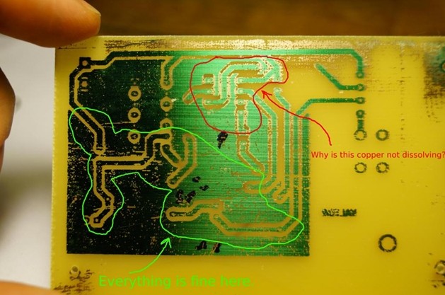
Inconsistent Etching Results
Etching inconsistencies arise from uneven application of etchant or variations in exposure time during the process. Over-etching can remove too much copper, breaking traces, while under-etching leaves unwanted copper, causing shorts. In multi-layer designs, this issue compounds as each layer must be etched separately before lamination, and errors on one layer affect the entire board.
Via Drilling and Connection Failures
Vias are small holes that connect different layers electrically. In home-etched boards, drilling vias manually often results in imprecise holes or burrs that prevent proper plating or soldering. Poor via connections lead to intermittent or complete signal loss, a critical concern in multi-layer PCB troubleshooting.
Delamination and Bonding Issues
Delamination occurs when layers separate due to weak bonding or contamination during lamination. This can happen if surfaces are not cleaned properly before pressing or if heat and pressure are unevenly applied. Delaminated boards lose structural integrity and electrical performance, posing a significant challenge in DIY PCB repair.
Solder Mask and Surface Defects
Applying solder mask at home can result in uneven coverage or air bubbles, exposing copper to oxidation or causing shorts during soldering. Surface defects also include scratches or contamination that interfere with component placement and soldering quality, impacting overall board functionality.
Practical Solutions for DIY PCB Repair and Troubleshooting
Addressing issues in home-etched multi-layer PCBs requires a blend of careful inspection and hands-on repair techniques. Here are practical steps to tackle common problems and improve outcomes in home electronics repair.
Step 1: Visual Inspection and Initial Diagnosis
Begin with a thorough visual inspection under good lighting or with a magnifying glass. Look for obvious signs of misalignment, etching errors, or delamination. Check for broken traces, uneven copper removal, or surface contamination. This initial step helps identify PCB etching problems before moving to electrical testing.
Step 2: Correcting Layer Misalignment
If misalignment is detected, it is often impossible to separate bonded layers without damage. Prevention is key here. Use registration holes or marks on each layer during design and align them precisely before bonding. For minor misalignments, carefully drill vias at corrected positions if feasible, though this requires precision tools and steady hands.
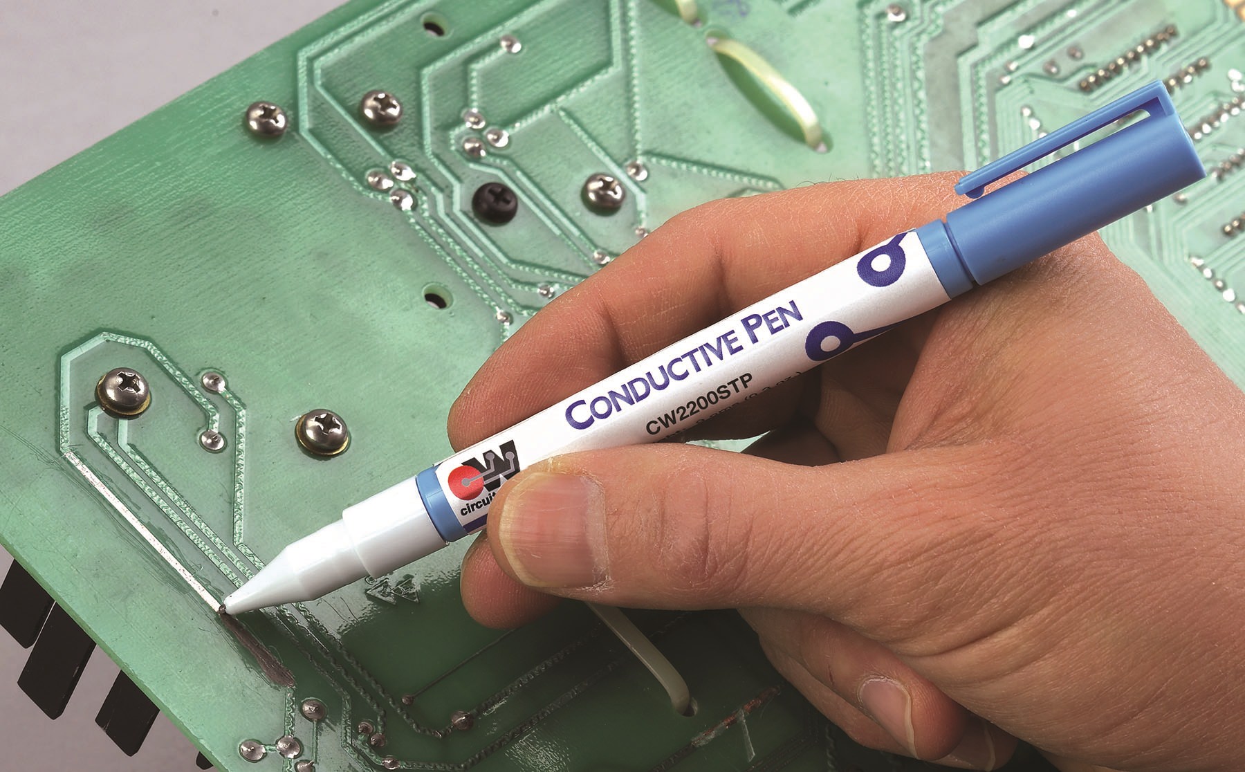
Step 3: Fixing Etching Inconsistencies
For over-etched traces, use a conductive pen or thin wire to bridge broken sections as a DIY PCB repair method. Secure the repair with epoxy to prevent movement. For under-etched areas, carefully remove excess copper with a fine-tip tool or reapply etchant to specific spots using a cotton swab. Always wear protective gear when handling chemicals.
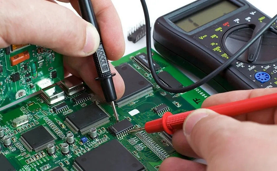
Step 4: Repairing Via Connection Issues
Poor via connections can often be fixed by re-drilling with a slightly larger bit to clear debris, followed by inserting a small wire or rivet to ensure conductivity. If plating is not an option at home, soldering a wire through the via can provide a temporary solution. Test continuity with a multimeter to confirm the fix.
Step 5: Addressing Delamination Problems
Delamination is challenging to repair once it occurs. If separation is minor, apply epoxy resin between layers and clamp the board under even pressure until cured. However, severe delamination usually means starting over. To prevent this, ensure all layers are clean and free of dust or grease before bonding, and apply consistent heat and pressure during lamination.
Step 6: Improving Solder Mask Application
For uneven solder mask, carefully remove the defective layer with isopropyl alcohol and a soft brush, then reapply a thin, even coat using a brush or stencil. Cure the mask under appropriate conditions, following the material’s guidelines. This step protects traces and enhances soldering precision in home electronics repair.
Suggested Reading: Multilayer PCB Repair: Challenges and Solutions for Complex Circuit Boards
Troubleshooting Workflow for Multi-Layer PCB Issues
A structured approach to multi-layer PCB troubleshooting saves time and reduces frustration. Follow this workflow to systematically address problems in home-etched boards.
- Power Off and Safety First: Always disconnect power before inspecting or repairing a PCB to avoid electrical hazards.
- Visual Check: Start with a detailed look at each layer for physical defects like cracks, burns, or misalignment.
- Continuity Testing: Use a multimeter to check for broken traces or failed vias between layers. Test key points based on the schematic.
- Component Isolation: Remove components if necessary to isolate board issues from part failures. Test the board independently.
- Repair and Retest: Apply fixes as described earlier, then retest for continuity and functionality. Repeat until issues are resolved.
This methodical process aligns with industry practices for diagnosing PCB issues, ensuring hobbyists tackle problems logically.
Preventative Tips for Successful Home-Etched PCBs
While troubleshooting and DIY PCB repair are essential skills, preventing issues during fabrication yields better results. Consider these tips to minimize problems in future projects.
- Design with Precision: Use software to create accurate layouts with clear registration marks for layer alignment.
- Control Etching Conditions: Maintain consistent etchant concentration and temperature. Avoid overexposure by timing the process carefully.
- Use Quality Materials: Opt for reliable substrates and copper-clad boards suitable for multi-layer designs to reduce bonding failures.
- Practice Cleanliness: Work in a dust-free environment and clean layers thoroughly before lamination to prevent contamination.
- Test Early and Often: Verify each layer’s integrity after etching and before stacking to catch errors early in the process.
Adopting these habits reduces the need for extensive home electronics repair and improves the reliability of multi-layer PCBs.
Conclusion
Home-etched multi-layer PCBs open up exciting possibilities for electronic hobbyists, but they come with a unique set of challenges. From layer misalignment to etching inconsistencies, understanding and addressing PCB etching problems is vital for successful projects. By following a structured approach to multi-layer PCB troubleshooting, applying practical DIY PCB repair techniques, and adopting preventative measures, hobbyists can overcome common issues and achieve reliable results. These skills not only save time and resources but also deepen your expertise in home electronics repair. With patience and practice, creating complex multi-layer designs at home becomes an achievable and fulfilling goal.
FAQs
Q1: What are the most common PCB etching problems in home-etched multi-layer boards?
A1: Common PCB etching problems include over-etching, which removes too much copper and breaks traces, and under-etching, leaving excess copper that causes shorts. Layer misalignment and uneven etchant application also frequently occur. These issues disrupt circuit functionality, especially in multi-layer designs where precision across layers is critical for proper signal routing.
Q2: How can I perform DIY PCB repair on a broken trace in a multi-layer board?
A2: For DIY PCB repair, use a conductive pen to draw over the broken trace and restore connectivity. Alternatively, solder a thin wire across the gap for a stronger fix. Secure the repair with epoxy to prevent movement. Test continuity with a multimeter to ensure the connection is reliable before reassembling the circuit.
Q3: What tools are essential for multi-layer PCB troubleshooting at home?
A3: Essential tools for multi-layer PCB troubleshooting include a multimeter for continuity testing, a magnifying glass for visual inspection, and a small drill for via repairs. Fine-tip soldering tools and conductive pens are also useful for trace fixes. These basic tools help identify and resolve issues without requiring advanced equipment.
Q4: How can I prevent delamination during home electronics repair of multi-layer PCBs?
A4: Prevent delamination in home electronics repair by ensuring all layers are clean before bonding. Remove dust and grease with isopropyl alcohol. Apply even heat and pressure during lamination to create a strong bond. Using quality materials and avoiding rushed processes further reduces the risk of layers separating over time.
References
IPC-6012E — Qualification and Performance Specification for Rigid Printed Boards. IPC, 2020.
IPC-A-600K — Acceptability of Printed Boards. IPC, 2020.


