Introduction
Microvias are essential components in modern high-density interconnect (HDI) printed circuit boards, enabling compact designs and improved signal integrity for advanced electronics. However, microvia PCB defects can compromise reliability, leading to costly failures in critical applications. Issues such as voiding, delamination, and plating problems often arise during fabrication or assembly, impacting performance. This guide, tailored for electric engineers, explores the root causes of microvia PCB troubleshooting challenges and provides practical solutions to address them. By understanding these common issues, engineers can enhance design and manufacturing processes to ensure robust PCB performance. The following sections will break down the technical aspects of microvia defects and offer actionable insights to mitigate risks effectively.
What Are Microvia PCB Defects and Why Do They Matter?
Microvias are small, laser-drilled vias typically less than 150 micrometers in diameter, used to connect layers in multilayer PCBs. They are critical for HDI designs, allowing higher component density and shorter signal paths. However, microvia PCB defects can disrupt electrical connectivity, thermal management, and structural integrity. Common issues include voiding within the via structure, delamination of surrounding materials, and plating inconsistencies that lead to weak connections.
These defects matter because they often result in signal loss, power delivery issues, or complete board failure. In industries like aerospace, automotive, and telecommunications, where reliability is paramount, even minor microvia flaws can have severe consequences. Addressing these problems early through effective microvia PCB troubleshooting saves time, reduces costs, and ensures compliance with stringent quality standards. Engineers must prioritize defect prevention and resolution to meet performance expectations in demanding applications.
Causes of Microvia PCB Defects
Understanding the root causes of microvia PCB defects is the first step in effective troubleshooting. These issues often stem from material properties, process parameters, or design constraints. Below are the primary mechanisms behind common problems like voiding, delamination, and plating issues.
Material and Design Factors
The choice of materials plays a significant role in microvia reliability. Low-quality dielectrics or laminates with poor thermal stability can lead to microvia PCB delamination under thermal stress. Similarly, mismatched coefficients of thermal expansion between layers cause mechanical strain, resulting in cracks or separation. Design errors, such as improper aspect ratios for microvias, can also hinder proper filling during plating, leading to voids or incomplete connections.
Fabrication Process Challenges
During manufacturing, several process variables contribute to microvia PCB defects. Laser drilling inconsistencies may create uneven via walls, trapping air or debris that results in microvia PCB voiding. Inadequate cleaning before plating can leave residues, preventing uniform copper deposition and causing plating issues. Additionally, improper lamination pressure or temperature can induce stress, leading to microvia PCB delamination between layers.
Assembly and Environmental Stress
Post-fabrication, assembly processes like reflow soldering expose PCBs to high temperatures, which can exacerbate existing microvia flaws. Thermal cycling may cause expansion and contraction, weakening via structures and resulting in cracks. Environmental factors, such as humidity, can also penetrate poorly sealed microvias, accelerating degradation and contributing to plating issues or delamination over time.
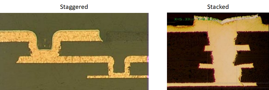
Common Microvia PCB Defects and Their Identification
Identifying microvia PCB defects early is crucial for effective troubleshooting. This section outlines the most frequent issues, their visual or measurable characteristics, and diagnostic methods.
Microvia PCB Voiding
Voiding occurs when air pockets or incomplete filling exists within the microvia structure. This defect often appears as dark spots or gaps in X-ray or cross-sectional imaging. Voiding weakens electrical conductivity and can lead to intermittent connections. It is commonly caused by trapped gases during plating or poor via wall preparation.
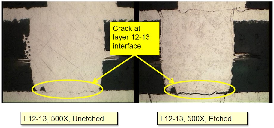
Microvia PCB Delamination
Delamination refers to the separation of layers or materials around the microvia, often visible as blisters or cracks under microscopic inspection. This issue arises from thermal stress, poor adhesion, or moisture ingress. Microvia PCB delamination compromises structural integrity and can disrupt signal paths.
Microvia PCB Plating Issues
Plating issues manifest as uneven or incomplete copper deposition inside the microvia, detectable through cross-sectional analysis or electrical testing. Thin or missing plating leads to high resistance or open circuits. Causes include inadequate cleaning, improper plating bath chemistry, or insufficient current density during electroplating.
Practical Solutions for Microvia PCB Troubleshooting
Resolving microvia PCB defects requires a systematic approach, combining design optimization, process control, and thorough inspection. Below are actionable strategies to address common issues.
Design Optimization
Start with design rules that minimize microvia stress. Use aspect ratios below 0.75:1 to ensure proper plating and filling, as recommended by widely recognized standards like IPC-2226. Select materials with compatible thermal expansion properties to reduce the risk of microvia PCB delamination. Incorporate sufficient annular rings around microvias to enhance mechanical stability.
Process Control in Fabrication
Tight control over fabrication processes is essential for defect prevention. Optimize laser drilling parameters to achieve smooth via walls, reducing the likelihood of microvia PCB voiding. Implement rigorous cleaning steps before plating to remove debris and ensure uniform copper deposition. Monitor lamination conditions to avoid excessive heat or pressure that could induce stress and delamination.
Advanced Plating Techniques
To tackle microvia PCB plating issues, consider pulse plating methods that improve copper distribution in high-aspect-ratio vias. Maintain strict control over plating bath composition and temperature to prevent defects. Regularly inspect plating thickness using cross-sectional analysis to confirm compliance with standards like IPC-6012E.
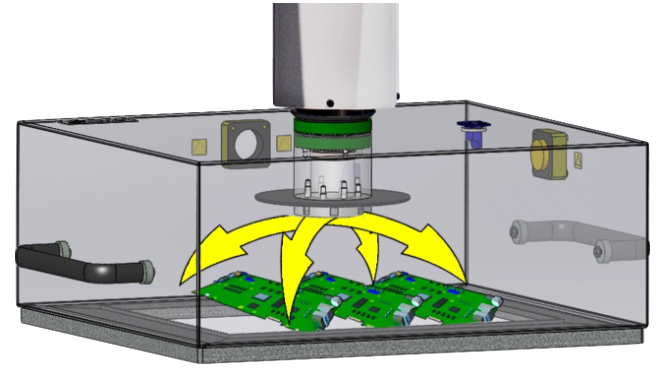
Inspection and Testing Protocols
Implement robust inspection protocols to catch defects early. Use automated optical inspection for surface-level issues and X-ray imaging for internal voiding. Conduct thermal cycling tests per IPC-TM-650 to assess reliability under stress. Electrical testing should verify continuity and resistance in microvia structures, ensuring no hidden plating issues remain.
Best Practices for Preventing Microvia PCB Defects
Prevention is always more efficient than troubleshooting after defects occur. Adopting best practices during design and manufacturing minimizes the risk of microvia PCB defects.
- Material Selection: Choose high-quality laminates and dielectrics with proven thermal and mechanical stability, adhering to guidelines in IPC-A-600K.
- Process Monitoring: Continuously monitor critical parameters like drilling speed, plating current, and lamination temperature to maintain consistency.
- Training and Standards Compliance: Ensure all personnel are trained in relevant standards, such as IPC-9121, which provides detailed troubleshooting guidance for fabrication processes.
- Regular Audits: Perform periodic audits of fabrication and assembly processes to identify potential sources of defects before they impact production.
Case Study: Resolving Microvia PCB Voiding in HDI Designs
In a typical HDI project, an engineering team encountered recurring microvia PCB voiding that led to signal integrity issues. Initial inspection using X-ray imaging revealed air pockets within the vias. The root cause was traced to inconsistent laser drilling, which left rough via walls, trapping gases during plating. By adjusting drilling parameters and introducing a post-drill cleaning step with plasma treatment, voiding was reduced significantly. Subsequent electrical tests confirmed improved connectivity. This case highlights the importance of process optimization and iterative testing in microvia PCB troubleshooting, aligning with practices outlined in IPC-9121.
Suggested Reading: Microvia PCB Design Rules: A Practical Handbook for Error Free HDI Layouts
Conclusion
Microvia PCB defects, including voiding, delamination, and plating issues, pose significant challenges in achieving reliable HDI designs. By understanding the causes, from material mismatches to process inconsistencies, engineers can implement targeted solutions through design optimization, strict process control, and thorough inspection. Adhering to established standards ensures consistent quality and performance. Effective microvia PCB troubleshooting not only resolves existing problems but also prevents future failures, supporting the development of robust electronics for critical applications. With these strategies, teams can navigate the complexities of microvia technology confidently.
FAQs
Q1: What are the primary causes of microvia PCB voiding in HDI designs?
A1: Microvia PCB voiding often results from trapped air or gases during plating, caused by rough via walls from inconsistent laser drilling. Poor cleaning before plating can also contribute. To mitigate this, optimize drilling parameters and ensure thorough cleaning processes. Following standards like IPC-9121 helps identify and address root causes during fabrication for reliable outcomes.
Q2: How can engineers prevent microvia PCB delamination in multilayer boards?
A2: Preventing microvia PCB delamination involves selecting materials with compatible thermal expansion properties and ensuring proper lamination conditions. Avoid excessive heat or pressure during manufacturing to minimize stress. Regular inspection for moisture ingress and adherence to IPC-A-600K guidelines can further reduce risks. Proper design and process control are essential for maintaining layer integrity.
Q3: What inspection methods are best for detecting microvia PCB plating issues?
A3: For detecting microvia PCB plating issues, X-ray imaging and cross-sectional analysis are highly effective in revealing uneven or incomplete copper deposition. Electrical testing can confirm continuity and resistance anomalies. Implementing these methods as per IPC-6012E standards ensures accurate identification of defects. Consistent monitoring during fabrication helps address plating problems before they escalate.
Q4: Why is microvia PCB troubleshooting critical for high-reliability applications?
A4: Microvia PCB troubleshooting is vital in high-reliability applications like aerospace or medical devices because defects can lead to signal loss or complete failure. Identifying issues like voiding or delamination early prevents costly rework and ensures performance. Standards such as IPC-TM-650 guide testing under stress conditions, helping engineers maintain quality in demanding environments.
References
IPC-6012E — Qualification and Performance Specification for Rigid Printed Boards. IPC, 2020.
IPC-A-600K — Acceptability of Printed Boards. IPC, 2020.
IPC-9121 — Troubleshooting for Printed Board Fabrication Processes. IPC, 2016.
IPC-2226 — Sectional Design Standard for High Density Interconnect (HDI) Printed Boards. IPC, 2003.
IPC-TM-650 — Test Methods Manual. IPC, 2021.


