Introduction
Power issues in printed circuit boards (PCBs) represent one of the most frequent failure modes encountered by electrical engineers during prototyping, assembly, and field service. These problems can manifest as intermittent operation, complete board failure, or degraded performance, often tracing back to the power delivery network (PDN). Effective PCB power supply troubleshooting requires a methodical approach to isolate root causes without introducing secondary damage. This article outlines a step-by-step diagnostic and repair process tailored for engineers, emphasizing tools like multimeters, oscilloscopes, and thermal cameras. By following these guidelines, teams can minimize downtime and enhance reliability in high-stakes applications such as power electronics and embedded systems. Mastering these techniques ensures compliance with industry benchmarks for board integrity.

Why PCB Power Issues Matter and Common Manifestations
PCB power problems disrupt the entire system's functionality because the PDN supplies stable voltage and current to all active components. Voltage instability leads to erratic behavior in microcontrollers, amplifiers, and sensors, while excessive current draw signals underlying faults like shorts. In production environments, unresolved power issues contribute to high failure rates, escalating costs for rework and scrap. Engineers must prioritize power rail verification early in the assembly process to catch defects before full system integration. Common symptoms include no power-up, flickering LEDs, overheating components, or unexpected resets. Addressing these systematically prevents cascading failures across interconnected modules.
Root Causes of PCB Power Failures
Short circuits often arise from solder bridges during surface-mount technology (SMT) assembly or inadvertent trace damage from mechanical stress. Voltage drops typically stem from undersized power traces, high-resistance vias, or poor solder joints that increase impedance in the current path. Power connector damage occurs due to insertion force, vibration, or environmental exposure, leading to intermittent contacts. Decoupling capacitor failures or improper grounding exacerbate noise on power rails, mimicking supply inadequacy. Manufacturing variances, such as inconsistent plating thickness per IPC-6012E standards, can introduce latent weaknesses. Environmental factors like thermal cycling further degrade connections over time.
Systematic Diagnosis: Step-by-Step PCB Power Supply Troubleshooting
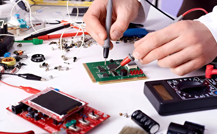
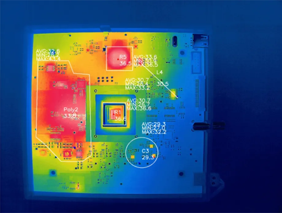
Begin with a powered-off visual inspection using a microscope to identify obvious defects like solder splatter or bent connector pins. Power on the board with a current-limited supply set to 10-20% above nominal voltage, monitoring total draw for anomalies exceeding expected idle current. Use a multimeter in diode mode to check for shorts between power and ground planes by probing accessible test points. For subtle issues, employ an oscilloscope to capture ripple on power rails, where excessive AC components indicate poor filtering. Thermal imaging helps localize hot spots indicative of partial shorts or high-resistance paths. Document findings in a fault tree to correlate symptoms with probable causes.
Diagnosing Short Circuits on PCBs
Short circuits demand immediate isolation to prevent component damage. Start by removing all loads and measuring continuity between VCC and GND nets; resistance below 1 ohm flags a hard short. Lift suspect components or cut traces minimally to sectionalize the board, retesting after each intervention. Solder wick or hot air removes bridges efficiently without excessive heat. Verify no multi-layer shorts by checking via continuity to inner planes. Post-repair, conform to J-STD-001 requirements for solder joint integrity to avoid recurrence.
Testing PCB Power Rails
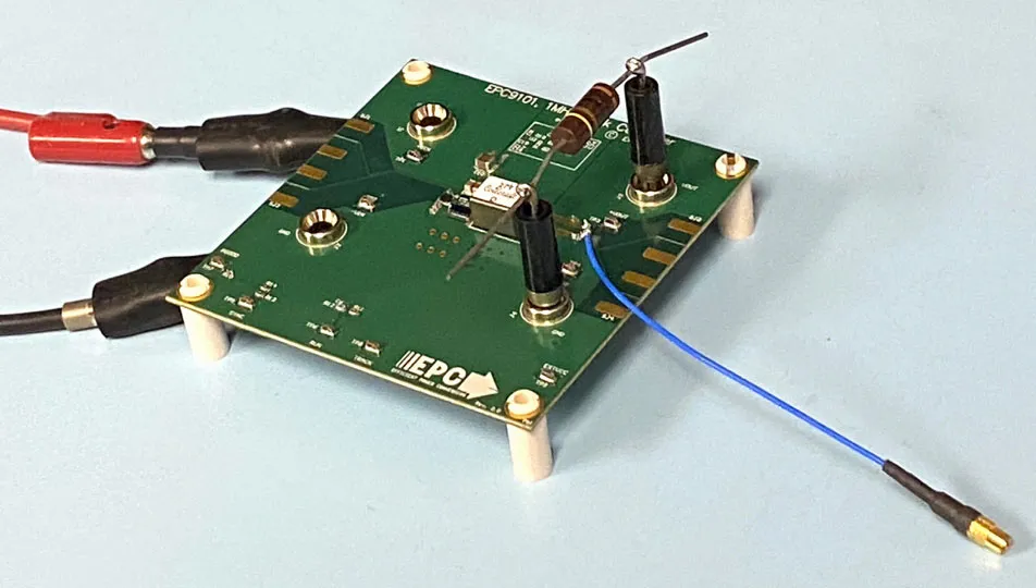
Power rail testing involves verifying voltage levels, ripple, and load response at multiple points. Apply nominal voltage at the input connector and measure drop across traces using a four-wire Kelvin connection for precision. Scope the rail under dynamic load to assess transient response; dips below 5% tolerance signal PDN weakness. Check bypass capacitors with an ESR meter for degradation. Map current distribution with a clamp meter on feeder lines. Ensure rail sequencing if multiple supplies are present, preventing latch-up in logic circuits.
Fixing Voltage Drops on PCBs
Voltage drops often result from trace resistance proportional to length, width, and material resistivity. Calculate expected drop using sheet rho of copper (approximately 0.5 mOhm per square for 1 oz foil) and compare to measurements. Widen traces or add stitching vias in redesigns, but for repairs, parallel jumper wires with adequate gauge mitigate immediate issues. Clean oxidized joints with isopropyl alcohol and reflow solder for better contact. Reinforce high-current paths with epoxy-filled wire bonds if board space allows. Validate fixes by loading the rail to maximum spec current and confirming less than 3% drop.
Repairing Power Connector Damage
Damaged connectors require careful extraction to avoid board delamination. Use a hot air station at 350°C with flux to desolder pins, supporting the board to prevent warpage. Inspect mounting holes for enlargement or cracking. Replace with compatible pitch and pin count, ensuring press-fit or through-hole retention per IPC-A-600K criteria. Apply conformal coating post-installation for environmental protection. Test continuity and insulation resistance after repair, cycling the connector 10 times to simulate use.
Advanced Techniques and Best Practices
Incorporate boundary scan or in-circuit testing during manufacturing to preempt power faults. Use finite element analysis for PDN simulation in design phase, optimizing decoupling placement. Maintain ESD-safe workstations to prevent static-induced latch-ups mimicking power issues. For multilayer boards, X-ray inspection reveals hidden via failures. Train teams on IPC workmanship standards to standardize repairs. Always bench-test repaired boards under accelerated stress before deployment.
Real-World Troubleshooting Insights
Consider a scenario where a power amplifier board fails to output full voltage. Initial current draw spikes to 2A idle, pointing to a short. Sectionalizing reveals a bridged SMD resistor on the 5V rail. After wick removal, voltage stabilizes, but ripple persists due to a cracked 0.1uF cap. Replacing it and adding extras resolves the issue. Oscilloscope confirms clean rails under 1kHz square wave load. This methodical isolation saved rework time and highlighted the need for automated optical inspection in assembly.
Conclusion
Troubleshooting PCB power issues demands precision, patience, and adherence to proven diagnostic flows. From diagnosing short circuits on PCBs to testing power rails and repairing connectors, a systematic approach minimizes risks and restores functionality efficiently. Engineers benefit from integrating visual, electrical, and thermal methods for comprehensive coverage. Prioritizing root cause analysis over symptom patching enhances long-term reliability. Implementing these practices aligns with industry standards, reducing failure rates in demanding applications. Regular training and tool calibration further empower teams for success.
FAQs
Q1: How do I start PCB power supply troubleshooting on a new assembly?
A1: Begin with a no-load power-up using a current-limited supply to detect shorts. Measure voltages at key rails against schematics, then scope for ripple. Visual checks for assembly defects precede functional tests. This sequence, per standard practices, isolates issues early without damage. Incorporate load steps gradually to verify stability. (52 words)
Q2: What are the signs of short circuits on PCBs and how to diagnose them?
A2: Excessive current draw, overheating, or no voltage on rails signal shorts. Use a multimeter for continuity between power and ground, then thermal imaging for hot spots. Sectionalize by lifting components or cutting traces temporarily. Diagnosing short circuits on PCBs this way prevents further harm and speeds repair. (48 words)
Q3: How can I fix voltage drops on PCBs effectively?
A3: Identify high-resistance paths via voltage measurements under load. Add parallel jumps or reflow joints to reduce impedance. Fixing voltage drops on PCBs requires verifying trace sizing and via quality. Retest with dynamic loads to confirm less than 5% deviation. (42 words)
Q4: What steps ensure reliable testing of PCB power rails after repair?
A4: Probe multiple points for DC accuracy and AC ripple with an oscilloscope. Apply rated loads and monitor transients. Testing PCB power rails includes ESR checks on caps and insulation resistance. Cycle power several times to validate stability. (40 words)
References
IPC-6012E — Qualification and Performance Specification for Rigid Printed Boards. IPC, 2017
J-STD-001H — Requirements for Soldered Electrical and Electronic Assemblies. IPC, 2018
IPC-A-600K — Acceptability of Printed Boards. IPC, 2020