Introduction
Copper cladding warpage in printed circuit boards (PCBs) is a significant concern for electrical engineers and manufacturers. This issue affects PCB flatness, leading to assembly challenges, compromised reliability, and potential failures in electronic devices. Warpage often stems from copper cladding stress, thermal stress in PCBs, and lamination defects during manufacturing. As modern electronics demand higher precision and smaller form factors, maintaining flatness becomes critical for ensuring performance. This article explores the root causes of PCB warpage related to copper cladding and offers practical prevention techniques. Aimed at electrical engineers, the content provides technical insights into material interactions, process controls, and industry standards to address these challenges effectively. By understanding these factors, professionals can mitigate risks and enhance board quality.
What Is Copper Cladding Warpage and Why It Matters
Copper cladding warpage refers to the deformation or bending of a PCB due to uneven stress distribution in the copper layers or substrate materials. Copper cladding, a fundamental component of PCBs, provides conductive pathways but can introduce mechanical stress if not balanced properly. This warpage disrupts PCB flatness, impacting the alignment of components during assembly and potentially causing soldering defects or mechanical failures.
The importance of addressing warpage cannot be overstated. In high-density interconnect designs, even slight deviations can lead to misalignment of fine-pitch components. This affects signal integrity and thermal management, critical for high-performance applications. Moreover, warpage increases the risk of stress fractures in solder joints, reducing the lifespan of the final product. For electrical engineers, recognizing and mitigating this issue ensures reliability and compliance with stringent industry standards.
Causes of Copper Cladding Warpage in PCBs
Material Imbalance and Copper Distribution
One primary cause of PCB warpage is the imbalance in copper distribution across the board layers. When copper density varies significantly between layers or within the same layer, it creates uneven mechanical stress. During thermal cycles, areas with higher copper density expand and contract differently compared to regions with less copper. This mismatch generates internal forces that warp the board.
Thermal Stress in PCB Manufacturing
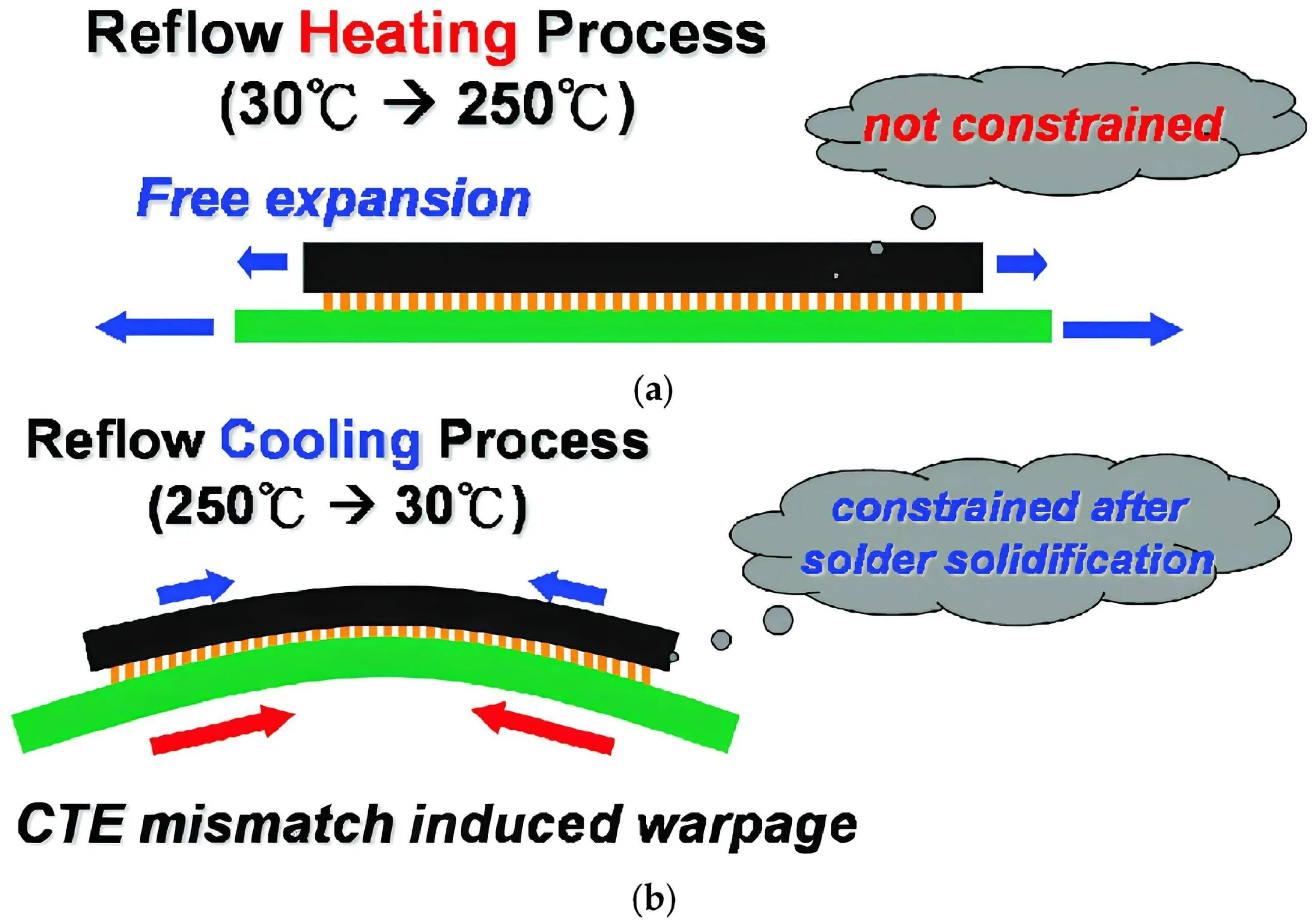
Thermal stress in PCBs arises during processes like lamination, soldering, and reflow. Copper and substrate materials, such as FR-4, have different coefficients of thermal expansion (CTE). When exposed to temperature changes, these materials expand or contract at different rates. If not managed, this discrepancy induces copper cladding stress, leading to warpage. High-temperature processes can exacerbate this issue if cooling is uneven or rapid.
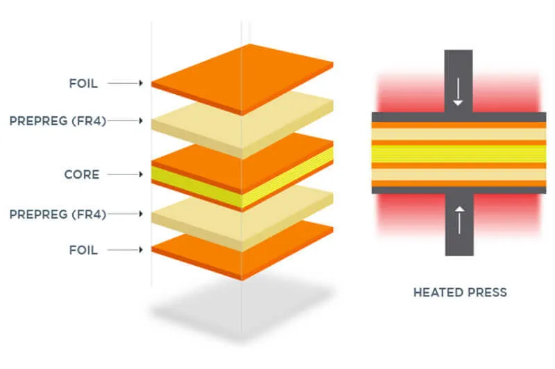
Lamination Defects and Process Variations
Lamination defects during fast turn PCB fabrication also contribute to warpage. Inconsistent pressure or temperature during the lamination process can result in uneven bonding between copper layers and the dielectric material. Voids, resin starvation, or improper curing may weaken the structural integrity, allowing stress to accumulate. Such defects often manifest as localized warpage, impacting overall board flatness.
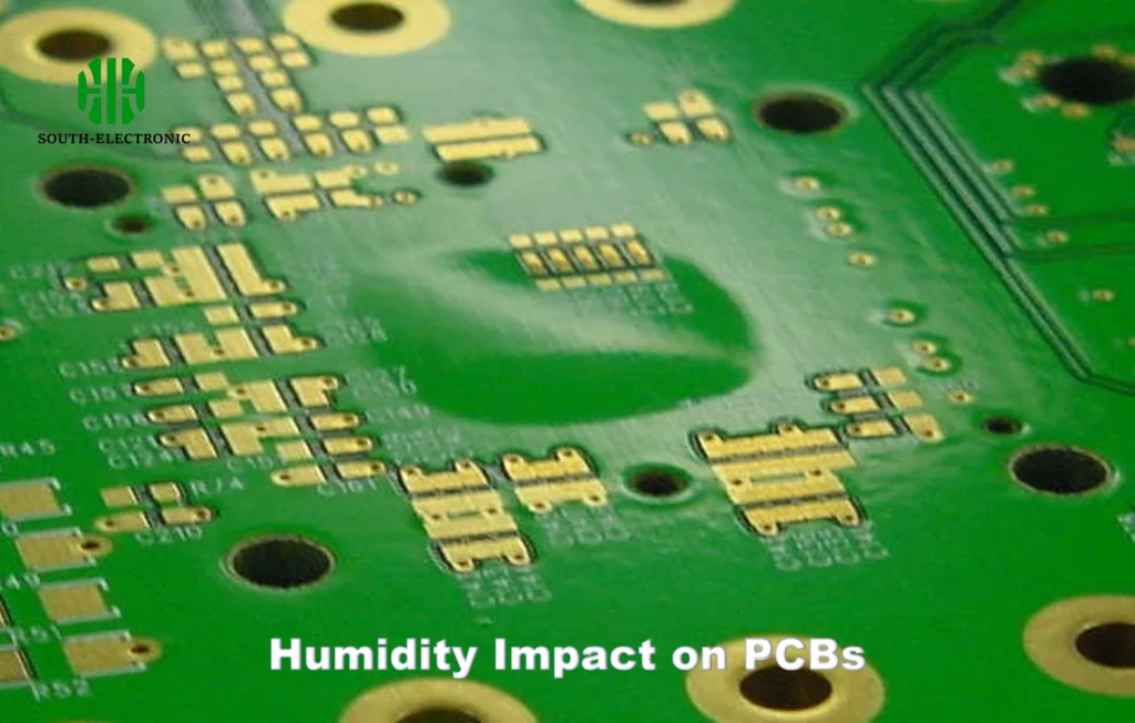
Moisture Absorption and Environmental Factors
Moisture absorption in the substrate material can worsen warpage. When a PCB absorbs moisture, the dielectric expands unevenly, creating additional stress against the copper cladding. Subsequent heating, such as during reflow, causes rapid moisture release, leading to delamination or further deformation. Environmental factors like humidity must be controlled to maintain stability.
Practical Solutions for Preventing Copper Cladding Warpage
Balanced Copper Distribution in Design
To prevent PCB warpage, engineers should prioritize balanced copper distribution during the design phase. Ensuring uniform copper density across layers minimizes differential stress. Dummy copper fills or grid patterns in low-density areas can help achieve this balance. Symmetry in stack-up design also reduces the likelihood of uneven expansion or contraction during thermal cycles.
Material Selection for CTE Compatibility
Selecting materials with compatible CTE values is essential. Matching the thermal expansion properties of copper and the substrate reduces stress at the interface. For high-temperature applications, consider low-CTE laminates or reinforced materials that offer better dimensional stability. Consulting material datasheets and adhering to industry standards ensures proper selection for specific use cases.
Optimized Lamination and Fabrication Processes
Controlling lamination parameters is critical to avoiding defects. Uniform pressure and temperature distribution during lamination ensure consistent bonding. Slow, controlled cooling after high-temperature processes prevents thermal shock. Implementing strict process controls, as outlined in standards like IPC-6012E, helps maintain quality and flatness throughout manufacturing.
Moisture Control and Storage Conditions
Preventing moisture absorption requires proper storage and handling. Storing PCBs in low-humidity environments and using desiccant packs can minimize exposure. Baking boards before PCBA assembly to remove absorbed moisture is a common practice. Following guidelines from standards like IPC-A-600K ensures boards remain in optimal condition prior to processing.
Testing and Inspection for Early Detection
Regular testing for warpage during production identifies issues early. Flatness measurements using precision tools, as recommended by IPC-A-600K, provide quantitative data on board condition. Shadow moiré or laser scanning techniques can map warpage profiles accurately. Early detection allows for corrective actions before assembly, saving time and resources.
Troubleshooting Warpage Issues in Manufacturing
For electrical engineers troubleshooting warpage, a systematic approach is necessary. Start by reviewing the design for copper balance and stack-up symmetry. Analyze fabrication reports for lamination process deviations or material inconsistencies. If warpage occurs post-assembly, assess thermal profiles during reflow to identify excessive stress points. Comparing measured flatness against acceptance criteria in IPC-A-600K ensures compliance. Adjusting material choices or process parameters based on findings can resolve recurring issues. Documenting each case builds a knowledge base for future prevention.
Conclusion
Copper cladding warpage poses a significant challenge in PCB manufacturing, driven by factors like copper imbalance, thermal stress, and lamination defects. Maintaining PCB flatness is vital for ensuring assembly accuracy and long-term reliability in electronic devices. By understanding the causes, such as material mismatches and process variations, engineers can implement effective prevention strategies. Balanced design, material compatibility, optimized fabrication, and rigorous testing align with industry best practices. Adhering to recognized standards enhances quality control, reducing the risk of warpage. Electrical engineers equipped with these insights can address challenges proactively, ensuring high-performance outcomes in their projects.
FAQs
Q1: What are the main causes of PCB warpage related to copper cladding?
A1: PCB warpage often results from uneven copper distribution creating mechanical stress. Thermal stress in PCBs, due to differing expansion rates between copper and substrate, also contributes. Lamination defects and moisture absorption further exacerbate the issue. Identifying these factors early through design reviews and process controls is essential for maintaining flatness.
Q2: How does thermal stress in PCBs affect copper cladding warpage?
A2: Thermal stress in PCBs occurs when copper and substrate materials expand differently under heat. During manufacturing or operation, this mismatch induces copper cladding stress, leading to deformation. Controlling temperature profiles and selecting compatible materials, as per industry standards, minimizes this effect and preserves board integrity.
Q3: What steps can prevent lamination defects causing PCB warpage?
A3: Preventing lamination defects involves uniform pressure and temperature during fabrication. Slow cooling after lamination avoids thermal shock. Strict adherence to process guidelines, like those in IPC-6012E, ensures consistent bonding. Regular inspection for voids or resin issues also helps maintain PCB flatness during production.
Q4: Why is PCB flatness critical for assembly and performance?
A4: PCB flatness directly impacts component alignment during assembly. Warpage can cause soldering defects or mechanical stress on joints, affecting reliability. In high-density designs, flatness ensures signal integrity and thermal management. Following standards like IPC-A-600K for flatness criteria supports optimal performance in final applications.
References
IPC-6012E — Qualification and Performance Specification for Rigid Printed Boards. IPC, 2020.
IPC-A-600K — Acceptability of Printed Boards. IPC, 2020.


