Introduction
Modern electronics demand ever-smaller form factors while maintaining functionality and performance. Double-sided PCBs address this challenge by enabling space-saving PCB design through the use of both board surfaces for components and traces. Unlike single-sided boards, they provide double-sided PCB advantages such as increased component density and flexible routing options, making them ideal for compact applications. Electrical engineers often select these boards to balance cost, complexity, and reliability in designs ranging from consumer devices to industrial controls. This article explores the structure, benefits, applications, and best practices for double-sided PCBs, offering structured insights grounded in engineering principles. By understanding their capabilities, designers can unlock innovative solutions for high-density electronics.
What Are Double-Sided PCBs and Why Do They Matter?
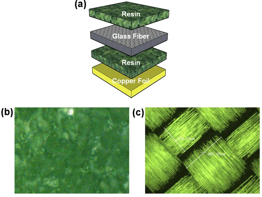
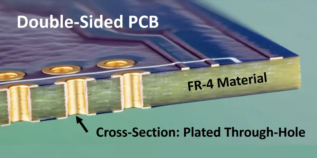
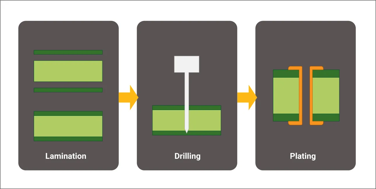
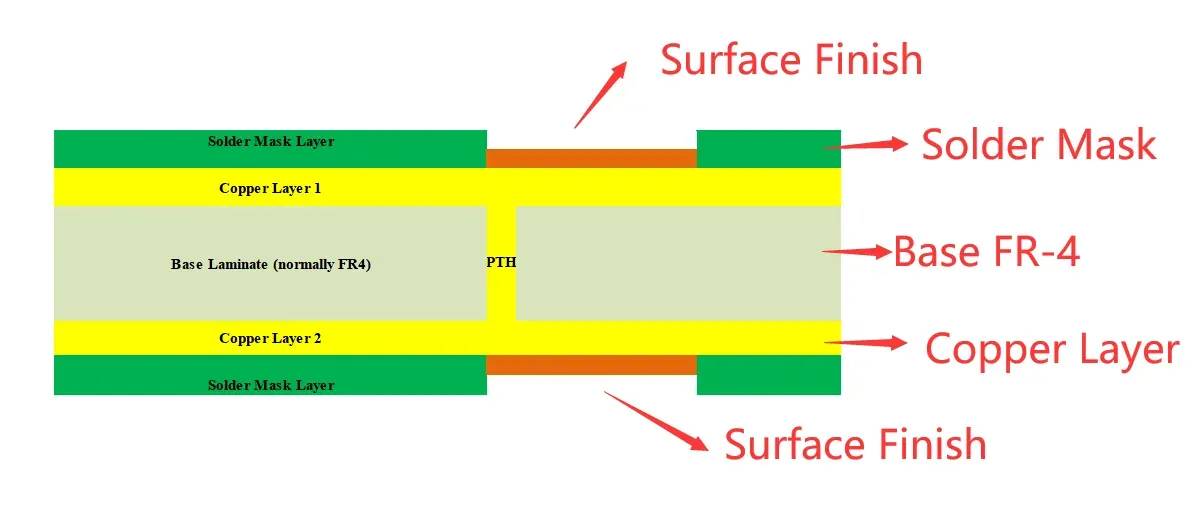
A double-sided PCB consists of a non-conductive substrate, typically with copper foil laminated on both the top and bottom surfaces. Conductive traces, pads, and vias connect circuits across these layers, allowing components to mount on either or both sides. This configuration contrasts with single-sided boards, which limit traces to one surface, restricting routing complexity. The manufacturing process involves imaging, etching, drilling, and plating to form plated through-holes (PTHs) that electrically link the sides.
Double-sided PCBs matter because they bridge the gap between simple single-sided boards and complex multilayers, supporting moderate circuit densities without excessive cost. They excel in space-saving PCB design, where board area must minimize while accommodating more interconnections. For electrical engineers, these boards offer a practical step-up in performance, enabling designs that fit stringent size constraints in portable and embedded systems. Their relevance grows with the miniaturization trend in electronics, where every square millimeter counts toward overall product efficiency.
Technical Principles of Double-Sided PCBs
The core principle of double-sided PCBs lies in the PTH, a drilled hole plated with copper to conduct signals between layers. The substrate, often a fiberglass-reinforced epoxy, provides mechanical support and electrical insulation between the copper layers. During fabrication, panels undergo dry film photoresist application, exposure, development, and etching to define trace patterns on both sides simultaneously or sequentially. Plating follows drilling to deposit copper inside holes, ensuring robust barrel integrity for current flow and mechanical strength.
Vias in double-sided boards are primarily through-hole types, spanning the full board thickness, which simplifies manufacturing compared to blind or buried vias in multilayers. Copper thickness, typically standardized for current-carrying capacity, influences thermal dissipation and signal integrity. Engineers must consider aspect ratios, defined as hole depth to diameter, to avoid plating voids that compromise reliability. Adherence to design guidelines ensures minimal crosstalk and controlled impedance in routed signals.
Signal routing leverages both layers for flexible routing options, allowing traces to cross under components or avoid congestion on one side. Ground and power planes can occupy one side fully, enhancing shielding and reducing noise. Thermal management benefits from dual-sided component placement, distributing heat sources evenly. These principles enable higher component density without transitioning to costlier multilayer stacks.
Key Advantages of Double-Sided PCBs
One primary double-sided PCB advantage is elevated component density, as both surfaces accommodate surface-mount or through-hole parts. This doubles the available real estate compared to single-sided designs, crucial for space-saving PCB design in constrained enclosures. Engineers can populate densely without overlapping traces, reducing board size by up to 50 percent in many layouts while maintaining functionality.
Flexible routing options represent another strength, permitting traces to weave between layers via vias, alleviating congestion and shortening signal paths. This reduces parasitic inductance and capacitance, improving high-frequency performance. Cost efficiency arises from simpler fabrication than multilayers, with fewer lamination cycles and inspection steps. Reliability remains high, as dual layers distribute mechanical stress during flexing or vibration.
Compared to single-sided boards, double-sided versions support more complex circuits like amplifiers or controllers without wire jumpers, which introduce failure points. They also facilitate easier prototyping, as standard processes apply universally. For moderate pin counts, they outperform single-sided in electrical performance without multilayer overhead.
Double-Sided PCB Applications
Double-sided PCBs find widespread use in consumer electronics, powering devices like remote controls, audio amplifiers, and LED drivers where compact size and affordability align. In automotive systems, they control dashboards, sensors, and lighting modules, enduring vibration and temperature swings through robust PTH connections. Industrial applications include power supplies, HVAC controllers, and instrumentation panels, benefiting from enhanced component density for feature-rich designs.
Medical devices leverage their space-saving PCB design for portable monitors and diagnostic tools, ensuring reliable interconnections in battery-powered units. Telecommunications equipment, such as routers and modems, employs double-sided boards for signal distribution across ports. Vending machines and UPS systems utilize them for control logic, combining flexible routing options with cost-effective production. These applications highlight versatility across sectors demanding balanced performance and economy.
Best Practices for Design and Manufacturing
Effective double-sided PCB design starts with layer planning: assign analog, digital, and power sections strategically to minimize crosstalk. Place vias judiciously to support flexible routing options, maintaining clearances per established guidelines. Simulate thermal profiles early, as dual-sided placement can create hotspots if heat sinks or vias for dissipation are overlooked. Optimize component orientation for automated assembly, grouping similar parts to streamline reflow processes.
Manufacturing follows IPC-6012E standards for qualification and performance of rigid printed boards, ensuring consistent plating and etch quality. Drill hole sizes must match aspect ratios below 10:1 to guarantee void-free barrels. Solder mask application protects traces on both sides, preventing shorts during assembly. Post-etch cleaning removes residues, enhancing IPC-A-600K acceptability criteria for surface finish and conductor integrity.
Assembly best practices include sequential soldering for mixed technology boards: reflow SMD on one side first, then wave or reflow the opposite. Inspect for warpage, as asymmetric populations stress the substrate. Test continuity and isolation thoroughly, verifying PTH reliability under load. These steps yield high-yield production aligned with engineering reliability goals.
Troubleshooting Common Challenges
Engineers often encounter via failures in double-sided PCBs due to plating inconsistencies or drill smear. Mitigate by specifying controlled depth drilling and desmear processes before electroless copper deposition. Component shadowing during reflow poses issues on densely populated sides; counter with low-profile parts and optimized stencil apertures.
Warpage from CTE mismatches between copper and substrate requires balanced copper distribution across layers. Signal integrity problems, like ground loops, resolve through dedicated ground planes on one side. Adopting IPC-2221 design principles early prevents routing errors, ensuring manufacturability.
Conclusion
Double-sided PCBs unlock compact designs by delivering double-sided PCB advantages like superior component density and flexible routing options. Their technical foundation in PTH vias and dual-layer routing supports diverse applications from consumer gadgets to industrial controls. Best practices in design and manufacturing, guided by industry standards, ensure reliability and performance. For electrical engineers pursuing space-saving PCB design, these boards offer an optimal balance of capability and economy, paving the way for innovative electronics.
FAQs
Q1: What are the main double-sided PCB advantages for electrical engineers?
A1: Double-sided PCB advantages include higher component density by utilizing both board surfaces, enabling space-saving PCB design in tight enclosures. Flexible routing options reduce trace lengths and congestion, improving signal integrity. They provide cost-effective complexity over single-sided boards without multilayer expenses, supporting moderate circuits reliably. Manufacturing aligns with standards like IPC-6012E for consistent quality.
Q2: How do double-sided PCBs improve component density?
A2: Double-sided PCBs boost component density by allowing surface-mount devices on top and bottom layers, doubling placement area versus single-sided. PTH vias interconnect circuits efficiently, freeing surface space. This supports intricate layouts in compact products like sensors or controllers. Engineers achieve denser packing while maintaining thermal and electrical margins through strategic placement.
Q3: What are common double-sided PCB applications?
A3: Double-sided PCB applications span consumer electronics such as amplifiers and LED systems, automotive controls, and industrial power supplies. They suit UPS units, HVAC panels, and medical portables needing balanced density and cost. Flexible routing options enable feature-rich designs in instrumentation and telecom gear. Reliability in vibration-prone environments makes them versatile.
Q4: How can flexible routing options benefit space-saving PCB design?
A4: Flexible routing options in double-sided PCBs allow traces to alternate layers via vias, avoiding overlaps and shortening paths. This optimizes board real estate for higher component density in constrained designs. Ground planes on one side enhance shielding, reducing noise. Proper via placement per design standards ensures manufacturability and performance.
References
IPC-6012E — Qualification and Performance Specification for Rigid Printed Boards. IPC, 2017
IPC-A-600K — Acceptability of Printed Boards. IPC, 2020
IPC-2221 — Generic Standard on Printed Board Design. IPC, 2012