Introduction
Printed circuit board (PCB) fabrication involves transforming raw materials into functional boards through processes like lamination, etching, and routing. One critical aspect influencing overall costs is the choice of board dimensions relative to standard panel sizes used in production. Electric engineers often focus on performance and functionality during design, yet overlooking standard PCB sizes cost implications can lead to unnecessary expenses. PCB panel utilization directly affects material waste minimization, as panels are typically processed in batches to share setup costs across multiple boards. By aligning designs with common panel dimensions, such as 18 by 24 inches, manufacturers achieve higher yields and lower per-unit costs. This article explores PCB fabrication cost drivers tied to dimensions and outlines practical PCB cost reduction strategies for engineers.
Standard panels provide a fixed working area after accounting for borders and tooling margins, making dimension optimization essential from the outset. Factory processes demand consistent handling, where non-standard sizes increase scrap rates and handling times. Engineers benefit from understanding how these factors interplay to make informed design decisions that balance performance with economics.
What Are Standard PCB Dimensions and Why Do They Matter?
Standard PCB dimensions refer to common board sizes that fit efficiently within fabrication panels without excessive customization. Typical panel sizes include 18 by 24 inches, 12 by 18 inches, 21 by 24 inches, and smaller variants like 9 by 12 inches. These dimensions arise from equipment capabilities in lamination presses and etching lines, where panels maximize throughput. Usable areas within panels are reduced by border clearances, often 0.5 inches around the perimeter for handling and fiducials, leaving approximately 16 by 22 inches available in an 18 by 24 inch panel.
The relevance stems from PCB material waste minimization during high-volume production. Poor panelization leaves unused copper-clad laminate as scrap, driving up material costs which constitute a significant portion of fabrication expenses. Standard PCB sizes cost advantages become evident when multiple identical or compatible boards tile the panel seamlessly. For instance, rectangular boards under 10 by 10 inches panelize effectively, allowing rotations or arrays to fill space.
Factory-driven insights reveal that deviations from these norms trigger additional tooling, such as custom routing paths or extended setup times. IPC-2221C provides generic guidelines for printed board design, including considerations for dimensions that support manufacturability. Engineers prioritizing these standards ensure designs align with production realities, reducing iterations and delays.
Key PCB Fabrication Cost Drivers Related to Dimensions
PCB fabrication cost drivers encompass material usage, processing time, and yield rates, all heavily influenced by board dimensions. Larger individual boards consume more laminate per unit, but if they underutilize panels, overall efficiency drops sharply. Conversely, small boards risk inefficient spacing if not arrayed properly, leading to higher scrap percentages. Border requirements and inter-board gaps, typically 0.1 to 0.2 inches for V-scoring or tab-routing, further dictate viable layouts.
Material costs scale with panel count, where suboptimal fitting necessitates more panels for the same quantity. Etching chemicals and plating solutions are consumed per panel, amplifying expenses for wasteful arrangements. Routing and scoring operations add time-based charges, especially for irregular shapes that complicate tool paths. Standard panel utilization mitigates these by standardizing workflows across production runs.
Handling and inspection also factor in, as oversized or oddly shaped panels strain equipment limits. IPC-6012F outlines qualification specifications for rigid printed boards, emphasizing dimensional stability post-fabrication to avoid warpage issues from poor panel design. Engineers must account for these drivers early to embed cost efficiency into the design phase.
Thermal expansion during lamination affects dimensional accuracy, underscoring the need for symmetric layouts within panels. Non-standard sizes often require unique fixtures, escalating setup fees that dwarf per-board savings.
Panel Utilization: The Core Mechanism for Cost Savings
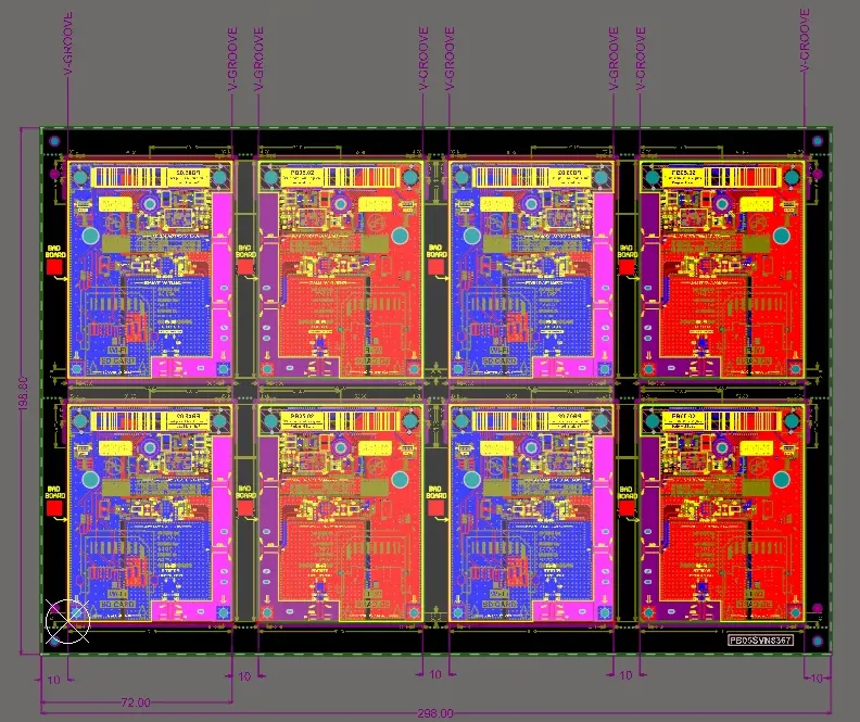
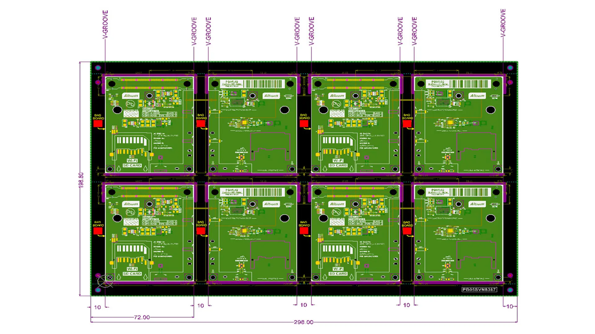
Panel utilization measures the percentage of panel area occupied by billable boards, directly tying to PCB material waste minimization. Optimal layouts achieve 80 to 90 percent usage by arranging boards with minimal gaps, often rotating orientations for tessellation. V-scoring suits straight-edged separations, while tab-routing handles complex contours with perforated tabs for depanelization. Factories prefer these methods on standard panels to streamline automated handling.
Common panels like 18 by 24 inches accommodate diverse board counts; for example, numerous small boards fit via dense arrays. Larger 21 by 24 inch panels suit mid-sized boards, balancing yield with rigidity. Usable areas exclude fiducial marks, tooling holes, and breakaway rails essential for alignment in pick-and-place and testing.
Inefficient utilization stems from ignoring panel constraints, such as forcing oversized boards that span multiple panels wastefully. PCB cost reduction strategies hinge on pre-production panelization simulations to predict yields. Collaboration with fabricators ensures layouts respect process tolerances, like minimum spacing to prevent scoring overlaps.
Multilayer boards demand wider borders due to alignment sensitivities, further emphasizing standard PCB sizes cost benefits. J-STD-001J criteria for soldered assemblies indirectly support efficient panelization by standardizing handling.
Practical Solutions and Best Practices for Engineers
Engineers can implement PCB cost reduction strategies by selecting dimensions compatible with standard panels from the schematic stage. Begin with board outlines under 12 inches wide to avoid custom tooling premiums. Use design software panelization features to test arrays on 18 by 24 inch templates, adjusting for 0.5 inch borders and 0.1 inch gaps.
Prioritize rectangular shapes over irregular contours, as they tile efficiently and simplify depanelization. For mixed-size runs, combine compatible boards on one panel to fill voids, enhancing overall yield. Rotate boards 90 degrees if it increases count without violating trace routing.
Specify V-scoring for high-volume straight separations, reserving tab-routing for shapes with internal cutouts. Include fiducials in corners per factory norms for optical alignment. Simulate warpage risks from asymmetric copper distribution, adhering to IPC-6012F performance specs.
Document panel layouts in Gerber files, noting array counts and methods. Prototype single panels before scaling to validate utilization. These steps minimize PCB fabrication cost drivers systematically.
Request quotes based on panel yield estimates, negotiating for standard sizes cost incentives. Iterative feedback loops with procurement refine future designs.
Factory Insights: Real-World Optimization Examples
In a typical factory scenario, a 4 by 6 inch board on an 18 by 24 inch panel yields about 12 units at 85 percent utilization with V-scoring. Adjusting to 5.5 by 5.5 inches via rotation boosts this to 14, trimming material needs. Such tweaks exemplify PCB panel utilization prowess without altering functionality.
For multilayer prototypes, 12 by 18 inch panels prove cost-effective, fitting test coupons alongside arrays. Tab-routing here allows flexible depanelization post-assembly. Engineers observe yield jumps from 70 to 90 percent by standardizing.
Challenges arise with high-aspect-ratio boards, where lengthwise orientation wastes edges. Flipping select units resolves this, a common factory-driven adjustment. These insights align with standards like IPC-2221C for manufacturable designs.
Conclusion
Standard PCB dimensions unlock substantial cost efficiencies by optimizing panel utilization and curbing waste. Key PCB fabrication cost drivers like material scrap and setup times diminish when designs match common panels such as 18 by 24 inches. Electric engineers adopting these PCB cost reduction strategies ensure economical production without compromising quality. Reference standards like IPC-6012F during design to maintain compliance. Proactive panelization planning delivers the most impact, fostering sustainable manufacturing practices.
FAQs
Q1: What are the main PCB cost reduction strategies tied to standard PCB sizes cost?
A1: Aligning board dimensions with standard panels like 18 by 24 inches maximizes yield per panel, sharing setup costs across more units. Rotate or array small boards to achieve 80-90 percent utilization, directly cutting material expenses. Avoid custom sizes that demand extra tooling, and collaborate on layouts early. This approach minimizes PCB fabrication cost drivers effectively.
Q2: How does PCB panel utilization contribute to material waste minimization?
A2: Efficient panel utilization fills usable areas, such as 16 by 22 inches on 18 by 24 panels, reducing scrap laminate. Proper spacing for V-scoring or tabs prevents overlaps while packing densely. Factories process full panels uniformly, so higher yields lower per-board chemical and handling costs. Engineers optimize via simulations for best results.
Q3: What are common standard PCB panel sizes and their impact on costs?
A3: Panels measure 18 by 24 inches, 21 by 24 inches, or 12 by 18 inches, with borders reducing usable space. These standards fit equipment, avoiding premiums for odd formats. Better fitting slashes panel counts needed, key to PCB cost reduction strategies. Larger panels suit volume runs for economies of scale.
Q4: Why do non-standard dimensions increase PCB fabrication cost drivers?
A4: They lead to poor panelization, generating more scrap and requiring custom fixtures or routings. Setup times extend for unique handling, inflating labor charges. Yield drops below 70 percent often, multiplying material use. Stick to standards for predictable, lower costs.
References
IPC-2221C — Generic Standard on Printed Board Design. IPC, 2023
IPC-6012F — Qualification and Performance Specification for Rigid Printed Boards. IPC, 2023
J-STD-001J — Requirements for Soldered Electrical and Electronic Assemblies. IPC, 2024