Introduction
Double-layer printed circuit boards (PCBs) are a cornerstone in modern electronics, offering a balance between complexity and cost for many applications. As designs grow denser with increasing component counts and shrinking footprints, effective via strategies become critical. Vias, the small conductive pathways connecting layers, play a vital role in ensuring signal integrity and power distribution. Poor via placement or incorrect via types can lead to electrical issues, manufacturing challenges, and reduced board reliability. This article explores the types of vias suitable for double-layer PCBs, optimal via placement techniques, and design considerations for high-density layouts. Aimed at electrical engineers, the content provides actionable insights to enhance PCB performance while adhering to industry standards. Let’s delve into the technical aspects of double-layer PCB vias and via design strategies.
What Are Double-Layer PCB Vias and Why Do They Matter?
Double-layer PCBs consist of two conductive layers, typically separated by an insulating substrate. Vias are essential to establish electrical connections between these layers, enabling signal routing and power delivery. In high-density designs, where space is limited, vias must be strategically placed to avoid interference with components and traces. The choice of via type and placement directly impacts signal quality, thermal management, and manufacturing feasibility. Incorrect via design can result in crosstalk, impedance mismatches, or drilling errors during production. For engineers, understanding double-layer PCB vias is crucial to meet performance goals and ensure the board can be reliably manufactured. With the rise of compact electronics, mastering via placement in PCB layouts is no longer optional but a fundamental skill for successful designs.
Technical Principles of PCB Via Types in Double-Layer Boards
Vias in double-layer PCBs are primarily categorized by their structure and function. Each type serves a specific purpose depending on the design requirements. Below are the main PCB via types relevant to double-layer boards, along with their characteristics.
Through-Hole Vias
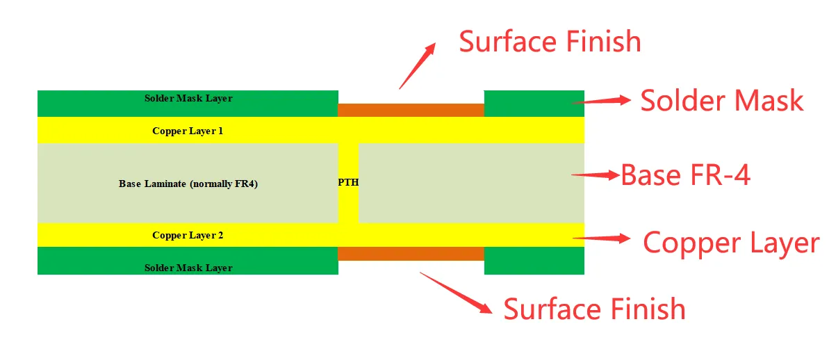
Through-hole vias extend through the entire thickness of the fast turn PCB, connecting both layers. They are the most common via type in double-layer designs due to their simplicity and ease of manufacturing. These vias are mechanically drilled and plated with conductive material to ensure connectivity. While reliable, through-hole vias consume space on both layers, which can be a limitation in high-density layouts. They are best suited for designs where space is not a critical constraint.
Suggested Reading: Through-Hole Vias: Essential Connections in Multilayer PCB Design
Via in Pad
Via in pad is a technique where vias are placed directly within the solder pads of surface-mount components. This approach is useful in high-density double-layer PCBs as it saves space on the board surface. However, it requires careful consideration during assembly to avoid solder wicking into the via, which can compromise joint quality. Special processes like via filling or capping may be needed to mitigate risks.
Stitching Vias
Stitching vias are multiple vias placed in a pattern to connect ground or power planes across layers. In double-layer PCBs, they help reduce electromagnetic interference by creating a low-impedance path for return currents. Stitching vias are often used near high-speed signal traces to maintain signal integrity. Their placement must be uniform to avoid uneven current distribution.
Understanding these via types is the foundation for effective PCB via design. Each type must be selected based on electrical needs, space constraints, and manufacturing capabilities. Industry standards like IPC-6012E provide guidelines on via dimensions and tolerances to ensure reliability.
Via Placement Strategies for High-Density Double-Layer PCBs
Via placement in PCB designs is as important as selecting the right via type. In high-density double-layer boards, improper placement can lead to signal degradation, thermal hotspots, or manufacturing defects. Below are key strategies to optimize via placement.
Minimize Via Count
Reducing the number of vias in a double-layer PCB helps save space and lowers manufacturing costs. Engineers should route traces on a single layer whenever possible before transitioning to the other layer through a via. This approach also reduces potential points of failure in the design.
Place Vias Away from High-Speed Traces
High-speed signals are sensitive to discontinuities caused by vias. Placing vias too close to these traces can introduce impedance mismatches and signal reflections. It is advisable to maintain a safe distance or use stitching vias to shield critical signals.
Distribute Vias for Thermal Balance
Vias conduct heat as well as electricity. In high-density designs, placing vias strategically can aid in dissipating heat from power-intensive components. Even distribution prevents localized thermal stress, which could lead to board warpage or component failure.
Align Vias with Manufacturing Grids
Manufacturing equipment often operates on specific grid alignments for drilling vias. Placing vias off-grid can result in drilling inaccuracies or increased production costs. Adhering to a grid-based layout ensures compatibility with standard processes as outlined in IPC-A-600K.
Avoid Vias Under Components
Placing vias directly under components, unless using via in pad, can complicate assembly and rework. Solder may flow into vias during reflow, leading to poor connections. Keeping vias clear of component footprints enhances reliability during production.
These via placement PCB strategies, when applied thoughtfully, can significantly improve the performance and manufacturability of high-density double-layer designs. Engineers must balance electrical requirements with physical constraints to achieve optimal results.
Best Practices for PCB Via Design in Double-Layer Boards
Designing vias for double-layer PCBs involves more than selecting types and placement. The following best practices ensure that via design contributes to overall board quality.
Adhere to Aspect Ratio Guidelines
The aspect ratio of a via, defined as the ratio of its depth to diameter, affects manufacturing reliability. A high aspect ratio can lead to incomplete plating inside the via, causing electrical failures. Standards like IPC-6012E recommend maintaining an aspect ratio below 10:1 for through-hole vias in double-layer boards.
Use Appropriate Via Sizes
Via diameter must be chosen based on current-carrying capacity and signal requirements. Smaller vias save space in high-density designs but may not handle high currents. Larger vias are more robust but consume valuable board area. Balancing these factors is essential for effective design.
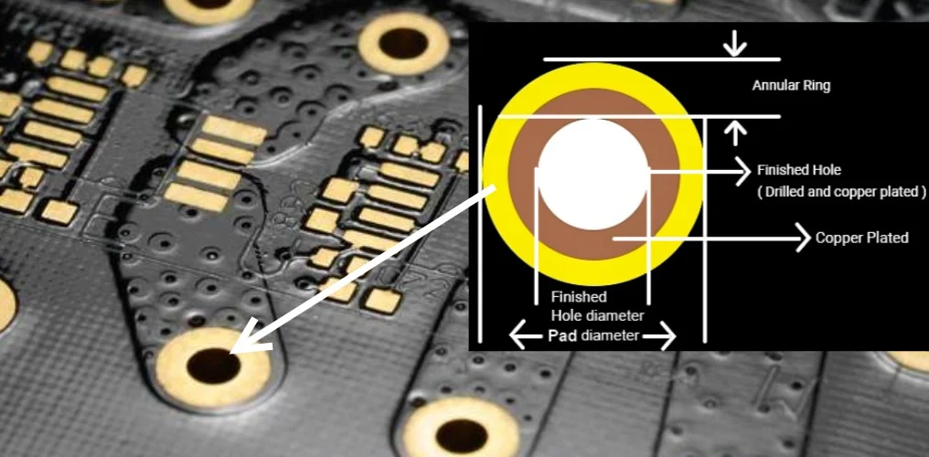
Implement Annular Ring Standards
The annular ring, the conductive pad surrounding a via, must meet minimum size requirements to ensure a strong connection. Insufficient annular ring width can lead to via breakage during thermal cycling. IPC-A-600K specifies acceptable annular ring dimensions for different via types.
Consider Via Filling for High-Density Layouts
In via in pad designs, filling vias with conductive or non-conductive material prevents solder wicking. This process adds cost but is often necessary for fine-pitch components in high-density layouts. It also improves thermal conductivity in some cases.
Following these practices during PCB via design ensures that double-layer boards meet both functional and manufacturing requirements. Engineers should consult relevant standards to validate their design choices.
Practical Insights for High-Density Double-Layer PCB Via Challenges
In real-world scenarios, engineers often face challenges unique to high-density double-layer PCBs. One common issue is routing congestion, where limited space makes it difficult to place vias without violating clearance rules. A practical solution is to prioritize critical signals and allocate vias for them first, then route less critical connections. Another challenge is maintaining signal integrity in mixed-signal designs. Using stitching vias around sensitive areas can create effective grounding, reducing noise. Thermal management also poses problems in compact layouts. Distributing vias near heat-generating components can help, but care must be taken to avoid creating current loops. These insights, derived from practical experience, complement standard guidelines and aid in overcoming design hurdles.
Conclusion
Effective via strategies are indispensable for high-density double-layer PCBs. Selecting the appropriate PCB via types, such as through-hole or via in pad, sets the foundation for a reliable design. Strategic via placement in PCB layouts minimizes signal issues and enhances thermal performance. Adhering to best practices in PCB via design, supported by industry standards, ensures manufacturability and durability. Electrical engineers must integrate these principles to meet the demands of modern electronics, where space and performance are paramount. By mastering double-layer PCB vias, designers can create robust boards that support increasingly complex applications with confidence.
FAQs
Q1: What are the main PCB via types used in double-layer boards?
A1: In double-layer PCBs, the primary via types include through-hole vias, which connect both layers through the board, and via in pad, used for space-saving in high-density designs. Stitching vias are also common for grounding and signal integrity. Each type serves specific purposes based on electrical and spatial needs, and selection must align with manufacturing capabilities.
Q2: How does via placement in PCB designs affect signal integrity?
A2: Via placement in PCB layouts significantly impacts signal integrity, especially for high-speed signals. Vias near critical traces can cause impedance mismatches and reflections. Placing vias away from such traces or using stitching vias for shielding helps maintain signal quality. Proper placement also reduces crosstalk and ensures reliable performance in dense designs.
Q3: What standards govern PCB via design for double-layer boards?
A3: PCB via design is guided by standards like IPC-6012E for performance specifications and IPC-A-600K for acceptability criteria. These documents outline rules for via dimensions, annular rings, and aspect ratios. Following these ensures manufacturability and reliability, helping engineers avoid common design pitfalls in double-layer PCB projects.
Q4: Why is via size important in double-layer PCB vias?
A4: Via size in double-layer PCB vias affects current capacity and space usage. Smaller vias save board area in high-density designs but may limit current handling. Larger vias support higher currents but reduce available routing space. Balancing size with electrical and layout requirements is crucial for optimal performance and manufacturability.
References
IPC-6012E - Qualification and Performance Specification for Rigid Printed Boards. IPC, 2020.
IPC-A-600K - Acceptability of Printed Boards. IPC, 2020.


