Introduction
Wave soldering remains a cornerstone in the assembly of through-hole PCB components, offering efficiency and reliability for high-volume production. For electrical engineers, optimizing PCB panel size during through-hole PCB assembly is critical to achieving consistent soldering quality and minimizing defects. This process directly impacts production costs, throughput, and product durability. In this article, we explore wave soldering techniques tailored for through-hole components, focusing on PCB panel optimization to ensure robust connections and streamlined manufacturing. By understanding the interplay between panel design, soldering parameters, and industry standards, engineers can enhance assembly outcomes. We will cover technical principles, best practices, and practical insights to help you navigate the complexities of wave soldering with confidence, ensuring your designs meet stringent quality requirements in every production run.
What Is Wave Soldering and Why It Matters
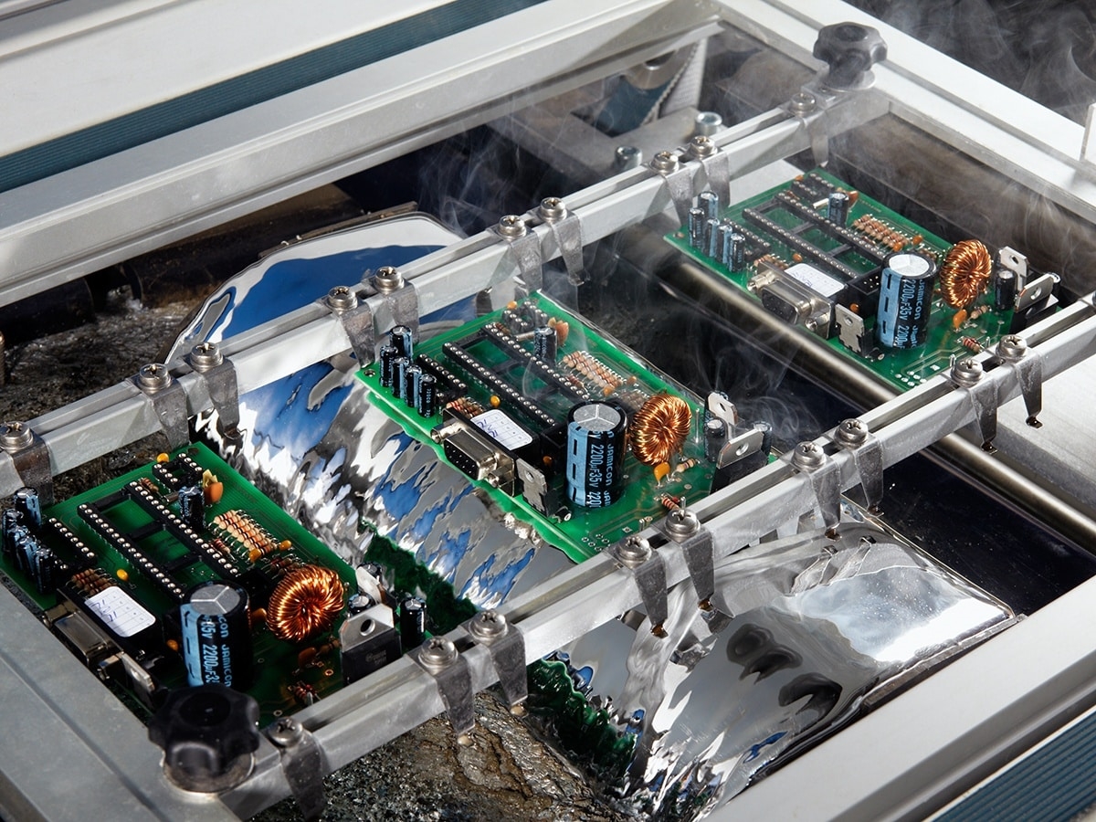
Wave soldering is a bulk soldering method used primarily for through-hole PCB assembly. It involves passing a PCB over a molten solder wave, which creates reliable electrical and mechanical connections between component leads and the board. This technique is ideal for high-volume manufacturing due to its speed and consistency. For electrical engineers, wave soldering matters because it addresses the need for durable joints in applications like power electronics and industrial controls, where through-hole components are often preferred for their mechanical strength. Poorly executed wave soldering can lead to defects such as insufficient solder fill or bridging, impacting product reliability. Optimizing PCB panel size plays a vital role in this process by ensuring uniform heat distribution and solder flow, reducing risks of warpage or uneven soldering across the board.
Related Reading: PCB Assembly and Soldering: Choosing the Right Soldering Technique
Technical Principles of Wave Soldering for Through-Hole Assembly
Wave soldering operates on fundamental principles of thermal dynamics and fluid mechanics. The process begins with flux application to clean and prepare the PCB surfaces for soldering. The board then passes through a preheat zone to minimize thermal shock before contacting the solder wave, typically maintained at temperatures aligned with industry guidelines like IPC-J-STD-001H. This standard outlines requirements for soldered electrical and electronic assemblies, ensuring proper wetting and joint formation.
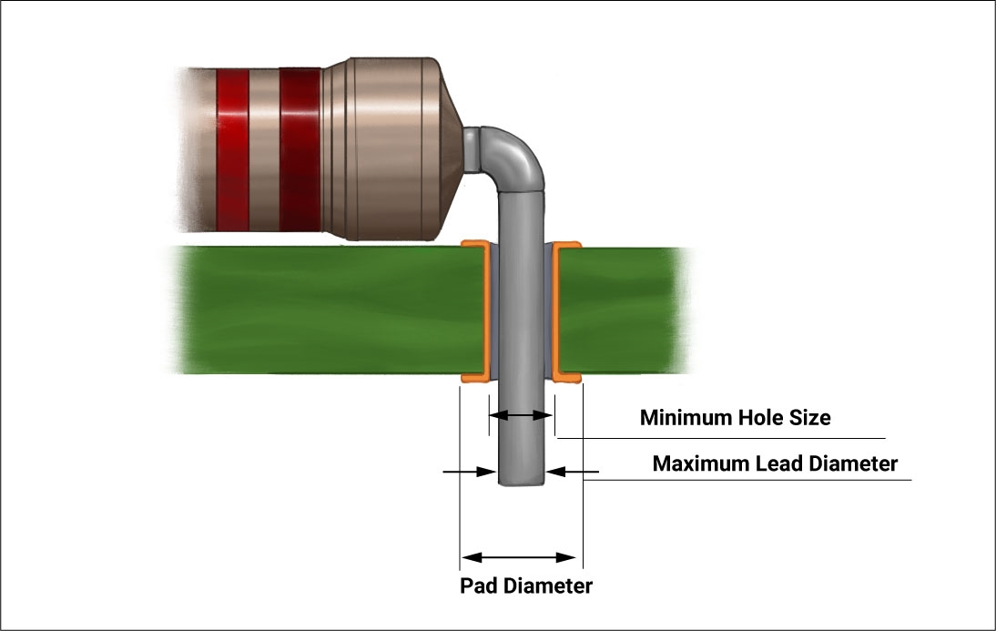
The solder wave, generated by a pump, contacts the bottom of the PCB, allowing capillary action to draw solder into the through-holes. For effective soldering, component leads must protrude adequately, and hole sizes must comply with standards such as IPC-A-600K, which specifies acceptability criteria for printed boards. Panel size influences thermal mass and heat dissipation, affecting preheat uniformity and solder wave interaction. Larger panels may retain heat unevenly, risking cold joints, while smaller panels might overheat, causing component stress. Engineers must balance panel dimensions with conveyor speed and solder temperature to maintain consistent results across the assembly.
PCB Panel Optimization for Wave Soldering
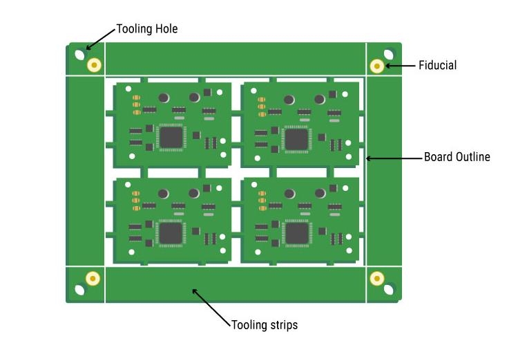
Optimizing PCB panel size is a critical factor in achieving efficient wave soldering for through-hole PCB assembly. Panel size affects not only thermal behavior but also manufacturing throughput and material usage. Below are key considerations for engineers when designing panels for wave soldering.
Balancing Panel Size with Thermal Uniformity
Larger panels can increase production efficiency by allowing more boards to be processed simultaneously. However, they also pose challenges in maintaining uniform temperature across the panel during preheating and soldering. Uneven heating can lead to warpage or incomplete solder joints. Standards like IPC-6012E, which governs rigid printed board performance, emphasize the importance of controlling thermal profiles to prevent such defects. Engineers should consider segmenting larger panels with strategic cutouts or adding dummy areas to balance heat distribution.
Component Layout and Orientation
Component placement on the panel significantly impacts wave soldering outcomes. Through-hole components should be oriented to minimize shadowing effects, where upstream components block solder flow to downstream leads. IPC-J-STD-001H provides guidelines for component spacing and orientation to ensure adequate solder penetration. Grouping components by size and type on the panel can also streamline soldering by reducing variations in thermal demand across the board.
Panel Edge Design and Support
Panel edges must be designed to withstand the mechanical stresses of conveyor systems during wave soldering. Adding support rails or breakaway tabs can prevent sagging or vibration, which might disrupt solder wave contact. Engineers should refer to IPC-A-600K for acceptable board edge conditions to avoid cracks or delamination. Properly designed edges also facilitate depanelization post-soldering without damaging assembled components.
Related Reading: PCB Panel Size Calculation: Enhancing Manufacturing Efficiency and Reducing Material Waste
Best Practices for Wave Soldering Techniques
Implementing effective wave soldering techniques ensures high-quality through-hole PCB assembly. Below are actionable practices for electrical engineers to enhance soldering outcomes while optimizing PCB panel size.
Flux Application and Control
Flux removes oxides from PCB surfaces and component leads, promoting solder wetting. Engineers must ensure even flux distribution across the panel, as inconsistent application can lead to poor joints. Foam or spray fluxing methods should be calibrated to avoid excess residue, which might contaminate the solder bath. Adhering to IPC-J-STD-001H guidelines helps maintain flux integrity during the process.
Preheat Settings for Panel Stability
Preheating minimizes thermal shock when the PCB contacts the solder wave. For larger panels, extended preheat times may be necessary to achieve uniform temperature. Monitoring thermal profiles, as recommended by IPC-6012E, ensures that the panel reaches the required temperature without exceeding component limits. This step is crucial for preventing warpage and ensuring solderability.
Solder Wave Height and Conveyor Speed
Adjusting the solder wave height and conveyor speed is essential for consistent soldering across the panel. A wave height that is too high can flood the board, causing bridging, while a low wave might result in insufficient solder fill. Conveyor speed must be optimized to allow adequate dwell time in the wave, especially for denser panels with numerous through-hole components. Standards like IPC-A-600K provide criteria for acceptable solder joint appearance.
Post-Soldering Inspection and Cleaning
After wave soldering, thorough inspection identifies defects such as cold joints or solder bridges. Visual and automated optical inspection methods should align with IPC-A-610H, which defines acceptability criteria for electronic assemblies. Cleaning removes flux residues to prevent corrosion, ensuring long-term reliability. Panel size impacts cleaning efficiency, as larger panels may require extended cleaning cycles to reach all areas.
Troubleshooting Common Wave Soldering Issues
Even with optimized PCB panel size and refined wave soldering techniques, challenges can arise during through-hole PCB assembly. Below are common issues and practical solutions for engineers to address them.
Insufficient Solder Fill in Through-Holes
This issue often results from inadequate preheat or poor wetting due to contamination. Ensure preheat settings align with component and board specifications per IPC-6012E. Verify flux activity and cleanliness of component leads and PCB surfaces. Adjusting wave height or dwell time can also improve solder penetration into through-holes.
Solder Bridging Between Pins
Bridging occurs when excess solder connects adjacent leads, often due to improper component spacing or wave height. Review PCB design against IPC-J-STD-001H for spacing requirements. Reducing wave height or adjusting conveyor speed can minimize excess solder accumulation. Using solder masks on critical areas of the panel further prevents bridging.
Thermal Stress and Component Damage
Larger panels or rapid temperature changes can induce thermal stress, damaging components. Implement gradual preheat and cooling profiles as per IPC-A-600K guidelines. Consider panel segmentation or adding thermal relief features to distribute heat evenly. Monitoring component datasheets for maximum temperature limits is also essential.
Conclusion
Wave soldering remains an indispensable technique for through-hole PCB assembly, offering efficiency and reliability in high-volume production. Optimizing PCB panel size is a pivotal aspect of this process, directly influencing thermal uniformity, solder quality, and manufacturing throughput. By adhering to industry standards such as IPC-J-STD-001H and IPC-A-600K, engineers can mitigate common defects like insufficient solder fill or bridging. Implementing best practices in flux application, preheat settings, and post-soldering inspection ensures consistent outcomes. With a clear understanding of wave soldering techniques and panel optimization, electrical engineers can achieve robust assemblies that meet the demands of modern electronics applications. Careful design and process control are the keys to soldering with confidence.
FAQs
Q1: How does PCB panel optimization impact wave soldering quality?
A1: PCB panel optimization directly affects wave soldering quality by ensuring uniform heat distribution and solder flow across the board. Larger panels may cause uneven heating, leading to defects like cold joints, while smaller panels risk overheating. Properly sized panels with strategic layouts, as per IPC-6012E guidelines, minimize warpage and improve joint reliability during through-hole PCB assembly.
Q2: What are the key wave soldering techniques for through-hole components?
A2: Key wave soldering techniques include precise flux application for surface preparation, controlled preheating to avoid thermal shock, and optimized solder wave height for consistent joint formation. Adjusting conveyor speed ensures adequate dwell time. Following IPC-J-STD-001H standards for process parameters and component spacing enhances soldering quality for through-hole PCB assembly.
Q3: Why is component orientation important in PCB panel design for wave soldering?
A3: Component orientation in PCB panel design prevents shadowing effects during wave soldering, where upstream components block solder flow to others. Aligning leads perpendicular to the wave direction ensures even contact. Adhering to IPC-A-600K for layout rules minimizes defects and ensures reliable solder joints in through-hole PCB assembly.
Q4: How can engineers prevent solder bridging during wave soldering?
A4: Engineers can prevent solder bridging by optimizing component spacing per IPC-J-STD-001H guidelines and adjusting solder wave height to avoid excess solder. Proper conveyor speed reduces dwell time issues. Using solder masks on critical panel areas further limits bridging risks during wave soldering of through-hole components.
References
IPC-J-STD-001H — Requirements for Soldered Electrical and Electronic Assemblies. IPC, 2021.
IPC-A-600K — Acceptability of Printed Boards. IPC, 2020.
IPC-6012E — Qualification and Performance Specification for Rigid Printed Boards. IPC, 2020.
IPC-A-610H — Acceptability of Electronic Assemblies. IPC, 2021.


