Introduction
In the realm of printed circuit board design, achieving high density and optimal performance is a constant pursuit for electrical engineers. Blind vias have emerged as a critical solution in multilayer PCB designs, offering unique advantages over traditional through hole vias. These specialized vias connect an outer layer to an inner layer without penetrating the entire board, enabling more efficient use of space and improved signal integrity. For engineers working on complex electronics, understanding the benefits of PCB blind vias is essential to creating compact, reliable, and high performing designs. This article explores the technical foundations, practical advantages, and best practices associated with blind vias in PCB design. By leveraging these components, engineers can address modern challenges in electronics, from miniaturization to enhanced functionality, while adhering to industry standards.
What Are Blind Vias and Why Do They Matter?
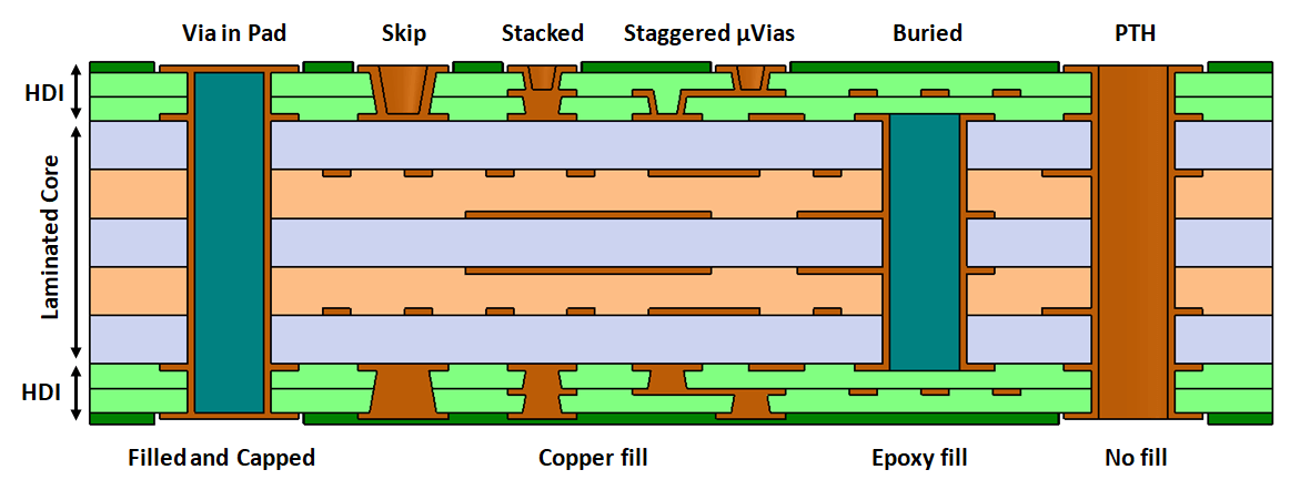
Blind vias are a type of interconnection in multilayer PCBs that link an external layer to one or more internal layers, without extending through the entire thickness of the board. Unlike through hole vias, which traverse all layers, blind vias terminate at a specific internal layer, preserving space on the opposite side of the board. This characteristic makes them invaluable in high density interconnect designs, where every square millimeter counts.
The importance of blind vias in PCB design lies in their ability to support miniaturization and complexity in modern electronics. As devices become smaller and more powerful, engineers face the challenge of fitting numerous components and connections into limited spaces. Blind vias address this by allowing denser routing and reducing the need for additional layers, directly impacting cost and performance. They are particularly relevant in applications like smartphones, medical devices, and aerospace systems, where compact and reliable designs are non negotiable.
Technical Principles of Blind Vias
The construction of blind vias involves advanced manufacturing techniques, often using laser drilling or controlled depth mechanical drilling to create precise holes that stop at a designated layer. These holes are then plated with conductive material, typically copper, to establish electrical connectivity between the outer and inner layers. The process requires strict adherence to standards such as IPC-6012E, which outlines the qualification and performance specifications for rigid printed boards, ensuring reliability and consistency in production.
One key principle behind blind vias is their role in reducing signal path length. By connecting directly to an internal layer, they minimize the distance a signal must travel compared to a through hole via, which can span unnecessary layers. This reduction is critical for high speed circuits, where shorter paths help maintain signal integrity and lower latency. Additionally, blind vias decrease the parasitic capacitance and inductance associated with longer vias, further enhancing electrical performance.
Another technical aspect is their impact on thermal management. Blind vias can be used to create thermal pathways, dissipating heat from critical components to internal copper planes. This capability is essential in designs with high power components, where overheating can degrade performance or cause failure. Engineers must carefully plan the placement and depth of these vias to optimize both electrical and thermal outcomes, often referencing guidelines from IPC-A-600K for acceptability criteria in printed boards.
Related Reading: Unlocking PCB Density: A Beginner's Guide to Blind Vias
Advantages of Blind Vias in PCB Design
The use of PCB blind vias offers several distinct advantages for electrical engineers tackling complex designs. Below are the primary benefits that make them a preferred choice in high density and high performance applications.
- Space Optimization: Blind vias free up space on the opposite side of the board since they do not penetrate through all layers. This allows for additional component placement or routing on the unused side, maximizing the use of available real estate.
- Improved Signal Integrity: By shortening the signal path, blind vias reduce delays and minimize electromagnetic interference. This is particularly beneficial in high speed digital circuits, where maintaining clean signals is critical.
- Reduced Layer Count: With blind vias, engineers can achieve denser connections without adding extra layers to the PCB stackup. Fewer layers translate to lower manufacturing costs and thinner boards, ideal for portable devices.
- Enhanced Design Flexibility: These vias enable more intricate routing patterns, allowing connections to be made precisely where needed. This flexibility is crucial when working with fine pitch components or ball grid arrays.
- Better Thermal Management: Strategically placed blind vias can transfer heat to internal planes, improving the thermal stability of the board. This helps protect sensitive components from thermal stress.
These advantages collectively contribute to more efficient and reliable PCB designs, addressing the evolving demands of modern electronics. Engineers can leverage these benefits to create products that meet stringent performance and size requirements, while ensuring compliance with standards like IPC-6012E for quality and durability.
Related Reading: Blind Vias in PCB Design: Optimizing High-Density Boards
Practical Applications of Blind Vias
Blind vias find extensive use in various industries where compact and high performance electronics are paramount. In consumer electronics, such as smartphones and tablets, they enable the dense packing of components within slim form factors. Medical devices, including wearable monitors and diagnostic equipment, rely on blind vias to integrate complex circuitry into small, portable units. Aerospace and automotive applications also benefit, as these sectors demand robust designs that can withstand harsh environments while maintaining minimal weight and size.
In high speed communication systems, blind vias play a crucial role in maintaining signal integrity across multiple layers. They are often used in server boards and networking equipment to handle rapid data transfer rates without degradation. Additionally, in power electronics, blind vias assist in managing heat dissipation, ensuring that high current components operate within safe temperature ranges.
When implementing blind vias, engineers must consider the manufacturing constraints outlined in standards like IPC-A-600K. This includes ensuring proper aspect ratios for drilling and plating, as well as verifying alignment accuracy during layer stacking. By adhering to these guidelines, the reliability and performance of the final product are safeguarded.
Best Practices for Implementing Blind Vias in PCB Design
To fully harness the benefits of PCB blind vias, electrical engineers should follow established best practices during the design and manufacturing phases. These guidelines ensure optimal performance and manufacturability while avoiding common pitfalls.
- Plan Layer Stackup Carefully: Determine the exact layers to be connected by blind vias early in the design process. This helps in optimizing the stackup and avoiding unnecessary complexity in manufacturing.
- Maintain Proper Aspect Ratios: Adhere to recommended aspect ratios for blind via drilling, typically outlined in industry standards like IPC-6012E. This ensures reliable plating and prevents defects during production.
- Use Simulation Tools: Employ signal integrity and thermal simulation software to predict the behavior of blind vias in the design. This can identify potential issues before fabrication begins.
- Collaborate with Fabricators: Engage with manufacturing teams to confirm the feasibility of blind via designs. Their input on capabilities and limitations can influence design decisions for better outcomes.
- Incorporate Test Points: Include accessible test points near blind vias to facilitate electrical testing and debugging. This practice aids in verifying connectivity and performance post fabrication.
By integrating these practices, engineers can mitigate risks associated with blind vias, such as drilling inaccuracies or plating failures. Compliance with standards like IPC-A-600K further ensures that the vias meet acceptability criteria, enhancing the overall quality of the PCB.
Challenges and Considerations
While blind vias offer significant advantages, they come with certain challenges that engineers must address. The manufacturing process for blind vias is more complex than for through hole vias, often requiring specialized equipment like laser drills. This can increase production costs, especially for small batch runs or prototypes. Additionally, the precision needed for alignment and depth control demands strict quality control measures, as outlined in standards such as IPC-6012E.
Another consideration is the potential for reliability issues if not designed or fabricated correctly. Poor plating or misalignment can lead to open circuits or weak connections, impacting the board's performance. Engineers must also account for the limited depth of blind vias, ensuring they are suitable for the specific layers they intend to connect.
To overcome these challenges, thorough design validation and close collaboration with fabrication partners are essential. Regular inspection and testing, guided by IPC-A-600K, can catch defects early, preventing costly rework or failures in the field.
Conclusion
Blind vias represent a powerful tool in the arsenal of electrical engineers working on multilayer PCB designs. Their ability to optimize space, enhance signal integrity, and support thermal management makes them indispensable in addressing the demands of modern electronics. By understanding the technical principles and adhering to best practices, engineers can unlock the full potential of PCB blind vias, creating compact and high performing designs. While challenges exist, careful planning and compliance with industry standards like IPC-6012E and IPC-A-600K ensure reliability and success. As technology continues to evolve, the strategic use of blind vias will remain a cornerstone of innovative PCB design, enabling the next generation of electronic devices.
FAQs
Q1: What are PCB blind vias and how do they differ from through hole vias?
A1: PCB blind vias connect an outer layer to an inner layer without passing through the entire board, unlike through hole vias that span all layers. This design saves space on the opposite side, allowing for denser layouts. They are ideal for high density PCB design, improving signal paths and reducing layer counts in complex electronics.
Q2: What are the key advantages of using blind vias in PCB design?
A2: The advantages of blind vias include space optimization, improved signal integrity, and reduced layer count. They enable denser routing and better thermal management in PCB design. This makes them suitable for compact devices, ensuring high performance while minimizing costs and maintaining compliance with industry standards.
Q3: How do blind vias impact the cost of PCB manufacturing?
A3: Blind vias can increase manufacturing costs due to the need for specialized processes like laser drilling and precise alignment. However, by reducing layer count, they may lower overall material expenses. Balancing design complexity with fabrication capabilities is crucial for cost effective PCB design using blind vias.
Q4: Are there specific standards for designing with PCB blind vias?
A4: Yes, standards like IPC-6012E for performance specifications and IPC-A-600K for acceptability criteria guide the design and manufacturing of PCB blind vias. These ensure proper drilling, plating, and alignment, maintaining reliability and quality in multilayer boards for various applications.
References
IPC-6012E — Qualification and Performance Specification for Rigid Printed Boards. IPC, 2020.
IPC-A-600K — Acceptability of Printed Boards. IPC, 2020.