Introduction
Copper plays a central role in printed circuit board (PCB) design and manufacturing, serving as the primary conductive material in electrical engineering PCB applications. Its thickness, often measured in microns, directly impacts current carrying capacity, thermal management, and overall board reliability. For electrical engineers, understanding copper properties and thickness requirements in microns is essential to optimize performance in various engineering applications. This article explores the significance of copper thickness, the material's inherent characteristics, and how these factors influence PCB design and functionality. By focusing on widely accepted industry standards and practical insights, this content aims to equip professionals with the knowledge needed to make informed decisions about this critical engineering material.
Why Copper Thickness Matters in PCB Design
Copper thickness in types of PCBs is a fundamental parameter that affects electrical and thermal performance. Measured in microns or ounces per square foot, it determines how much current a trace can carry without overheating or failing. In electrical engineering PCB contexts, selecting the appropriate copper thickness ensures signal integrity, minimizes power loss, and prevents thermal stress. Thinner copper layers, often around 17.5 microns (equivalent to 0.5 oz/ft2), are common in high density interconnects where space is limited. Thicker layers, such as 70 microns (2 oz/ft2), are used in power electronics to handle higher currents. Choosing the right thickness is a balance between performance needs and manufacturing constraints, making it a critical consideration for engineers working on diverse engineering applications.
Copper Properties Relevant to Electrical Engineering
Copper stands out as the preferred conductive material in PCB design due to its exceptional electrical and thermal conductivity. Its resistivity is approximately 1.68 micro ohm centimeters at room temperature, ensuring minimal energy loss during current flow. Additionally, copper's thermal conductivity allows it to dissipate heat effectively, protecting components from thermal damage. The material also exhibits good ductility, enabling it to be formed into thin layers without cracking during manufacturing. However, engineers must account for copper's tendency to oxidize, which can degrade performance if not properly managed with surface finishes. These copper properties make it indispensable in electrical engineering PCB designs, where reliability and efficiency are paramount for various engineering applications.
Key Properties of Copper
- Electrical conductivity: Ensures efficient current flow with low resistance.
- Thermal conductivity: Facilitates heat dissipation from critical components.
- Ductility: Allows thin layer formation without structural failure.
- Oxidation susceptibility: Requires protective coatings to maintain performance.
Understanding Copper Thickness in Microns
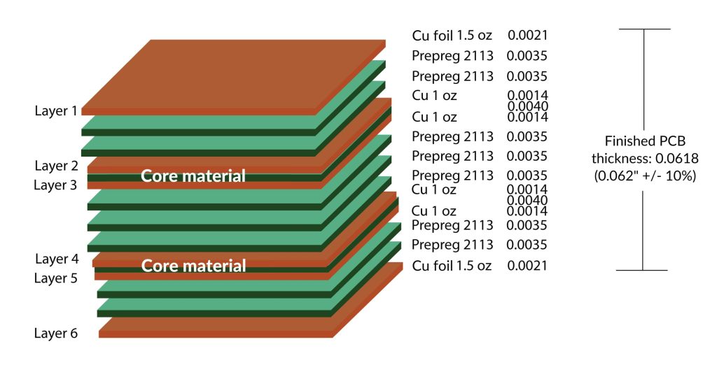
In PCB manufacturing, copper thickness is often specified in ounces per square foot, but converting to microns provides a more precise metric for engineers. One ounce per square foot translates to approximately 35 microns. Common thicknesses include 17.5 microns (0.5 oz/ft2), 35 microns (1 oz/ft2), 70 microns (2 oz/ft2), and 105 microns (3 oz/ft2). These values align with industry standards for different applications. For instance, high frequency circuits may use thinner copper to reduce skin effect losses, while power supplies demand thicker layers for higher current capacity. Electrical engineers must select thickness based on current requirements, board space, and thermal constraints to ensure optimal performance in their designs.
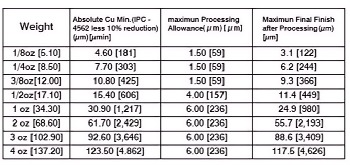
Conversion Table for Copper Thickness
- 0.5 oz/ft2 — 17.5 μm
- 1.0 oz/ft2 — 35.0 μm
- 2.0 oz/ft2 — 70.0 μm
- 3.0 oz/ft2 — 105.0 μm
Technical Principles Behind Copper Thickness Selection
Selecting the appropriate copper thickness involves understanding current carrying capacity and thermal dissipation. According to industry guidelines like those in IPC 2221B, trace width and copper thickness must be calculated based on the expected current and allowable temperature rise. Thicker copper reduces resistance, allowing higher currents without excessive heating. However, it increases board weight and cost while potentially complicating manufacturing. Thinner copper suits compact designs but risks overheating if current exceeds capacity. Engineers must also consider impedance control in high frequency applications, where copper thickness affects signal integrity. Balancing these factors ensures reliability in electrical engineering PCB projects.
Thickness Requirements for Different Engineering Applications
Copper thickness requirements vary across engineering applications due to differing electrical and mechanical demands. In consumer electronics, where space is limited, thinner copper layers around 17.5 to 35 microns are typical to support fine pitch components. Automotive and industrial applications often require 70 microns or more to handle higher currents and ensure durability under harsh conditions. High power systems, such as those in renewable energy, may use even thicker copper to manage substantial loads. Adhering to standards like IPC 6012E helps engineers specify thickness based on performance class and application needs, ensuring the chosen engineering material meets reliability expectations.
Application Based Thickness Guidelines
- Consumer electronics: 17.5 to 35 microns for compact, low power designs.
- Automotive systems: 70 microns for robustness and moderate current.
- Industrial power: 105 microns or higher for heavy duty current handling.
Practical Solutions for Copper Thickness Optimization
Electrical engineers can optimize copper thickness by following a systematic approach. First, define the current requirements using tools aligned with IPC 2221B to calculate minimum trace dimensions. Second, consider thermal management needs by simulating heat dissipation under load conditions. Third, evaluate manufacturing constraints, as thicker copper may require specialized processes. Finally, test prototypes under real world conditions to validate design choices. Adjusting thickness in specific board areas, such as using heavier copper on power traces and lighter on signal traces, can also enhance performance without increasing overall cost. These practices ensure effective use of this critical engineering material.
Challenges with Copper Thickness in PCB Manufacturing
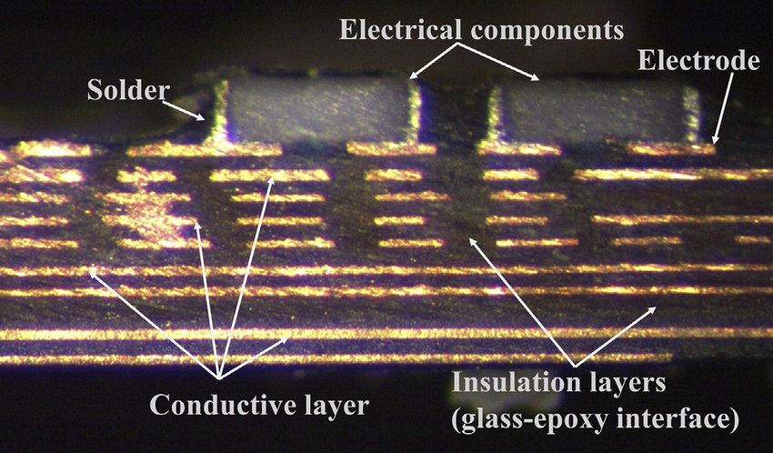
Managing copper thickness presents several challenges in PCB mass production. Uniformity across the board is vital, as variations can lead to inconsistent electrical performance. Thicker copper layers may cause etching difficulties, affecting trace precision. Additionally, lamination issues can arise if the copper thickness is not compatible with the dielectric material, risking delamination. Engineers must work within tolerances specified by standards like IPC A 600K to ensure quality. Addressing these challenges requires close attention to process control and material selection during the design phase of electrical engineering PCB projects.
Conclusion
Copper thickness in microns is a pivotal factor in PCB design, influencing current capacity, thermal performance, and manufacturing feasibility. By understanding copper properties and adhering to thickness requirements, electrical engineers can create reliable and efficient designs for diverse engineering applications. Standards such as IPC 2221B and IPC 6012E provide essential guidance for selecting the appropriate copper thickness based on application needs. With careful consideration of these principles, engineers can optimize their use of this vital engineering material, ensuring robust performance in every project they undertake.
FAQs
Q1: How does copper thickness in microns affect electrical engineering PCB performance?
A1: Copper thickness directly impacts current carrying capacity and heat dissipation in electrical engineering PCB designs. Thicker layers, such as 70 microns, support higher currents without overheating, while thinner layers like 17.5 microns suit compact, low power applications. Selecting the right thickness ensures signal integrity and prevents thermal issues, aligning with performance needs.
Q2: What are the key copper properties for engineering applications?
A2: Copper properties critical for engineering applications include high electrical conductivity for efficient current flow and thermal conductivity for heat dissipation. Its ductility allows thin layer formation, but oxidation susceptibility requires protective finishes. These traits make copper ideal for reliable and effective PCB designs across various industries.
Q3: How do thickness requirements vary across different engineering material uses in PCBs?
A3: Thickness requirements for copper as an engineering material vary by application. Consumer electronics often use 17.5 to 35 microns for space efficiency. Automotive and industrial systems require 70 microns or more for durability and higher currents. Power intensive applications may need 105 microns to manage substantial loads safely.
Q4: What standards guide copper thickness selection in electrical engineering PCB projects?
A4: Industry standards like IPC 2221B and IPC 6012E guide copper thickness selection in electrical engineering PCB projects. IPC 2221B provides formulas for current capacity based on thickness and trace width. IPC 6012E outlines performance specifications, ensuring designs meet reliability and quality criteria for specific applications.
References
IPC 2221B — Generic Standard on Printed Board Design. IPC, 2012.
IPC 6012E — Qualification and Performance Specification for Rigid Printed Boards. IPC, 2020.
IPC A 600K — Acceptability of Printed Boards. IPC, 2020.


