Introduction
The rapid deployment of 5G technology has transformed telecommunications, enabling faster data rates, lower latency, and enhanced connectivity. At the core of this revolution lies the printed circuit board (PCB), specifically designed to handle high-frequency signals. For electrical engineers, achieving optimum 5G performance hinges on meticulous layer stackup design. This aspect directly impacts signal integrity, impedance control, and overall system reliability. A well-planned 5G PCB stackup ensures minimal signal loss and interference, critical for high-speed applications. This article explores the principles of layer stackup design tailored for 5G, focusing on thicker copper layers, impedance control, and adherence to industry standards. By understanding these elements, engineers can create robust designs that meet the stringent demands of modern wireless communication systems.
What is Layer Stackup in 5G PCB Design and Why It Matters
Layer stackup refers to the arrangement of conductive and insulating layers within a multilayer PCB. In the context of 5G PCB design, stackup is pivotal because it determines how signals propagate through the board at high frequencies. 5G operates in millimeter-wave bands, often exceeding 24 GHz, where signal integrity becomes highly sensitive to layer configuration. A poorly designed stackup can lead to signal degradation, crosstalk, and electromagnetic interference, all of which undermine performance.
The importance of stackup design lies in its ability to support impedance control and minimize losses. For 5G applications, maintaining consistent impedance across traces is essential to prevent reflections that disrupt data transmission. Additionally, the stackup influences thermal management and mechanical stability, both vital for devices operating under high power and environmental stress. Engineers must prioritize symmetry, material selection, and layer sequencing to ensure the PCB meets the rigorous demands of 5G networks.
Technical Principles of Layer Stackup Design for 5G Performance
Signal Integrity at High Frequencies
Signal integrity is the cornerstone of 5G PCB performance. At high frequencies, signals are prone to attenuation due to dielectric losses and skin effect in copper traces. The skin effect causes current to concentrate near the conductor's surface, increasing resistance. To counter this, thicker copper layers are often used in critical signal paths. These layers reduce resistive losses and improve current-carrying capacity, essential for maintaining signal strength over long traces.
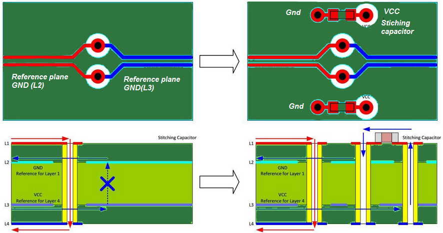
Furthermore, the dielectric material between layers plays a significant role. Low-loss dielectrics with stable permittivity across frequencies help preserve signal integrity. The stackup must position high-speed signal layers adjacent to continuous ground planes to minimize loop inductance and provide a stable return path. This configuration reduces electromagnetic interference and crosstalk, common challenges in densely packed 5G designs.
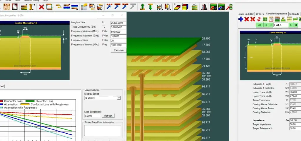
Impedance Control and Layer Arrangement
Impedance control is a critical parameter in 5G PCB design. It ensures that the characteristic impedance of transmission lines matches the source and load, preventing signal reflections. Stackup design directly affects impedance by determining the distance between signal layers and reference planes, as well as the dielectric constant of insulating materials. Engineers calculate impedance using trace width, layer thickness, and material properties, adhering to precise tolerances.
A typical 5G PCB stackup may include multiple signal layers interleaved with ground and power planes. This arrangement provides shielding and stabilizes impedance. Symmetry in the stackup is also crucial to avoid warpage during manufacturing and operation. For instance, placing signal layers equidistant from the board's center helps maintain mechanical balance while optimizing electrical performance.
Role of Thicker Copper Layers
Thicker copper layers are often integrated into 5G PCB designs to address high-frequency challenges. Copper thickness, typically measured in ounces per square foot, impacts both electrical and thermal performance. In high-power 5G applications, thicker copper reduces resistive heating and enhances current distribution. This is particularly important for power amplifier circuits and antenna feeds, where high current density is common.
Moreover, thicker copper improves signal integrity by lowering conductor losses at millimeter-wave frequencies. However, engineers must balance this with manufacturing constraints, as excessively thick copper can complicate etching processes and increase costs. A common practice is to use thicker copper selectively on power and ground layers while maintaining thinner copper on signal layers for precision.
Practical Solutions for Optimum 5G PCB Stackup Design
Layer Configuration Strategies
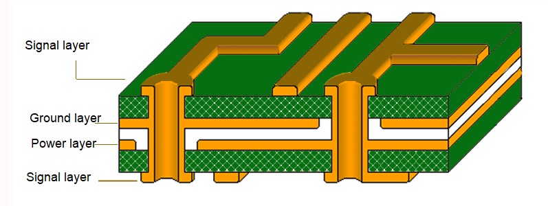
Designing a stackup for 5G performance involves strategic layer sequencing. A typical multilayer stackup might start with a signal layer on top, followed by a ground plane, then additional signal layers, power planes, and more ground planes. Ground planes act as shields, reducing crosstalk between adjacent signal layers. For high-density designs, microvias and buried vias can connect layers without compromising space, a technique often used in 5G devices.
Symmetry remains a guiding principle. An asymmetrical stackup can lead to mechanical stress, causing the board to warp under thermal cycles. Engineers should distribute copper and dielectric layers evenly across the board's thickness. Additionally, placing high-speed signals closer to the top or bottom layers can simplify routing while maintaining proximity to reference planes for impedance control.
Material Selection for High-Frequency Performance
Material choice is integral to 5G PCB stackup design. Dielectric materials must exhibit low dissipation factor and stable dielectric constant at high frequencies to minimize signal loss. Commonly, materials with low-loss characteristics are selected for critical layers. The dielectric thickness between signal and ground layers also affects impedance, requiring precise control during manufacturing.
Copper foil roughness is another consideration. Smoother copper reduces signal attenuation at high frequencies by minimizing skin effect losses. Engineers often collaborate with manufacturing teams to specify copper treatments that balance performance with producibility. Adherence to industry standards ensures that materials meet the necessary electrical and mechanical properties for 5G applications.
Adhering to Industry Standards
Compliance with recognized standards is non-negotiable in 5G PCB design. Standards such as IPC-6012E provide guidelines for rigid PCB qualification and performance, including layer stackup tolerances. Similarly, IPC-2221B offers design principles for establishing impedance control and layer configurations. These standards help engineers define stackup parameters that ensure reliability and manufacturability.
Thermal and mechanical testing standards, such as those outlined in IPC-TM-650, are also relevant. They provide methods to evaluate stackup stability under operating conditions typical of 5G environments. By aligning designs with these standards, engineers can mitigate risks of signal integrity issues and structural failures in the field.
Troubleshooting Common Stackup Issues in 5G Designs
Even with careful planning, 5G PCB stackup designs can encounter issues. Signal integrity problems often arise from mismatched impedance due to inconsistent dielectric thickness or trace geometry. Engineers can address this by using simulation tools to model impedance before fabrication. Adjusting layer spacing or trace widths based on simulation results helps achieve the desired performance.
Another common issue is thermal imbalance caused by uneven copper distribution across layers. This can lead to warpage or delamination. To prevent this, engineers should ensure uniform copper fill in unused areas and verify symmetry in the stackup. Ground pours in empty spaces also aid in heat dissipation and reduce electromagnetic interference, enhancing overall reliability.
Crosstalk between high-speed signals is a frequent concern in dense 5G layouts. Spacing signal traces adequately and ensuring continuous ground planes between layers can mitigate this. If crosstalk persists, revising the stackup to add extra shielding layers may be necessary, though this increases board thickness and cost.
Conclusion
Layer stackup design is a fundamental aspect of achieving optimum 5G performance in PCB applications. By prioritizing signal integrity, impedance control, and the strategic use of thicker copper layers, engineers can create boards that meet the high-frequency demands of 5G technology. Careful layer arrangement, material selection, and adherence to industry standards ensure reliability and efficiency in real-world conditions. As 5G continues to evolve, mastering stackup design remains essential for developing cutting-edge communication systems. Through systematic approaches and rigorous testing, electrical engineers can overcome challenges and deliver robust solutions for next-generation networks.
FAQs
Q1: How does layer stackup impact signal integrity in 5G PCB designs?
A1: Signal integrity in 5G PCB designs is heavily influenced by layer stackup. Proper arrangement of signal and ground layers minimizes crosstalk and electromagnetic interference. Proximity to reference planes ensures stable return paths, reducing signal loss at high frequencies. A well-designed stackup, adhering to industry standards like IPC-2221B, preserves data transmission quality essential for 5G performance.
Q2: Why are thicker copper layers important for 5G PCB performance?
A2: Thicker copper layers in 5G PCB designs reduce resistive losses and improve current capacity, vital for high-power circuits. They also enhance signal integrity by lowering conductor losses at millimeter-wave frequencies. While beneficial, their use must balance with manufacturing constraints to avoid etching issues. This approach supports robust performance in demanding 5G applications.
Q3: What role does impedance control play in 5G PCB stackup design?
A3: Impedance control is critical in 5G PCB stackup design to prevent signal reflections. It ensures transmission lines match source and load impedance, achieved through precise layer spacing and dielectric properties. Standards like IPC-6012E guide engineers in maintaining consistency. Effective impedance control is essential for reliable high-speed data transfer in 5G systems.
Q4: How can engineers optimize layer stackup for 5G applications?
A4: Engineers can optimize layer stackup for 5G by ensuring symmetry, using low-loss dielectrics, and placing signal layers near ground planes. Incorporating microvias aids in high-density designs, while adhering to standards like IPC-2221B ensures manufacturability. Simulation tools help predict performance, allowing adjustments in layer configuration for peak signal integrity and reliability.
References
IPC-6012E — Qualification and Performance Specification for Rigid Printed Boards. IPC, 2020.
IPC-2221B — Generic Standard on Printed Board Design. IPC, 2012.
IPC-TM-650 — Test Methods Manual. IPC, 2021.
ISO 9001:2015 — Quality Management Systems. ISO, 2015.


