What Role Does Copper Weight Play in PCB Design?
Printed circuit boards (PCBs) form the foundational structure for modern electronic devices, and a crucial decision for engineers involves selecting the appropriate copper weight. Copper weight, typically quantified in ounces per square foot (oz/ft²), directly influences a PCB’s ability to conduct electrical current, manage heat, and ensure overall reliability. The two most common options, 1oz and 2oz copper, each present distinct advantages and compromises. This discussion will explore the differences between these two copper weights, compare their current-carrying capacities, and offer practical advice to guide engineers in making informed design choices.
Whether you are designing a low-power microcontroller circuit or a robust high-current power supply, a thorough understanding of copper weight is essential for optimizing both performance and cost. Let's examine the technical specifics, contrast the two options, and highlight key considerations for your upcoming PCB projects.
Related Reading: What You Need to Know About Copper Weight in PCB Design
How Do 1oz and 2oz Copper Differ in PCBs?
Copper weight refers to the thickness of the copper foil integrated into a PCB, expressed as the mass of copper evenly distributed over one square foot. This measurement directly correlates with the foil's physical thickness.
Understanding Copper Thickness Equivalents
● 1oz copper: This signifies 1 ounce of copper per square foot, which is approximately equivalent to a thickness of 1.37 mils (0.0348 mm or 34.8 µm).
● 2oz copper: This indicates 2 ounces of copper per square foot, roughly equivalent to a thickness of 2.8 mils (0.070 mm or 70 µm).
A thicker copper layer provides a larger cross-sectional area, enhancing its capacity to carry electrical current and dissipate heat more effectively. However, increased copper thickness also generally leads to higher manufacturing costs and can introduce complexities in designs requiring fine-pitch components. Engineers must carefully balance these factors based on the specific requirements of their project.
How Does Copper Weight Impact Current-Carrying Capacity?
The current-carrying capacity of a PCB trace is determined by its cross-sectional area (influenced by copper weight and trace width), the permissible temperature rise, and environmental elements such as airflow and the board material itself. Let's compare the capacities of 1oz and 2oz copper, referencing industry standards like IPC-2221.
Current Capacity of 1oz Copper
Given its thinner profile, 1oz copper traces have a more limited current-carrying capacity. According to IPC-2221, a 10-mil-wide trace made with 1oz copper can typically carry about 1 ampere (A) with an allowable 10°C temperature rise. For a wider 50-mil trace, this capacity increases to approximately 2.6A under the same conditions. These figures are based on standard FR-4 material and typical ambient temperatures.
1oz copper is generally suitable for most applications involving low to moderate power, such as:
● Digital circuits, like those found in microcontrollers, where currents are typically below 1A.
● Interface ports (e.g., USB 2.0 traces carrying less than 500mA).
● Low-power LED circuits, handling currents up to 1A for multiple LEDs.
However, for applications requiring higher currents, 1oz copper might necessitate significantly wider traces, which can consume valuable board space and add complexity to the design.
Current Capacity of 2oz Copper
With its doubled thickness, 2oz copper offers a considerably higher current-carrying capacity. A 10-mil-wide trace made with 2oz copper can manage approximately 2A with a 10°C temperature rise, while a 50-mil-wide trace can carry around 4.8A. This makes 2oz copper an excellent choice for high-power applications, including:
● Power supplies and converters, especially those with currents exceeding 5A.
● Automotive electronics, such as motor drivers that might draw between 10-50A.
● Components for solar panels and inverters, where currents can reach up to 100A with appropriate design.
The increased cross-sectional area of 2oz copper reduces electrical resistance, which in turn minimizes voltage drops and heat generation. This allows 2oz copper to support higher currents without requiring excessively wide traces, thereby preserving valuable board space.
How Does Copper Weight Influence Thermal Management?
Copper weight also plays a vital role in thermal management. Thicker copper layers conduct heat more effectively, reducing the formation of localized hot spots and improving the overall reliability of the board.
Thermal Performance Comparison
● 1oz Copper: With a thermal conductivity of approximately 385 W/m-K, 1oz copper offers sufficient heat dissipation for low-power circuits. However, in scenarios involving high currents, its limited thickness can lead to substantial temperature increases, potentially pushing components or the FR-4 substrate beyond their safe operating limits (which is typically 130°C for standard materials).
● 2oz Copper: The doubled thickness of 2oz copper effectively halves its thermal resistance compared to 1oz copper. This allows it to distribute heat more efficiently across the board. This advantage is particularly valuable in power electronics, where components like MOSFETs or IGBTs generate considerable heat. For instance, a 2oz copper plane can reduce peak temperatures by 10-20°C compared to a 1oz plane under similar current loads.
In environments with elevated temperatures, such as automotive or aerospace applications, the superior thermal performance of 2oz copper can significantly extend component lifespan and help prevent thermal runaway.
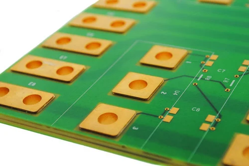
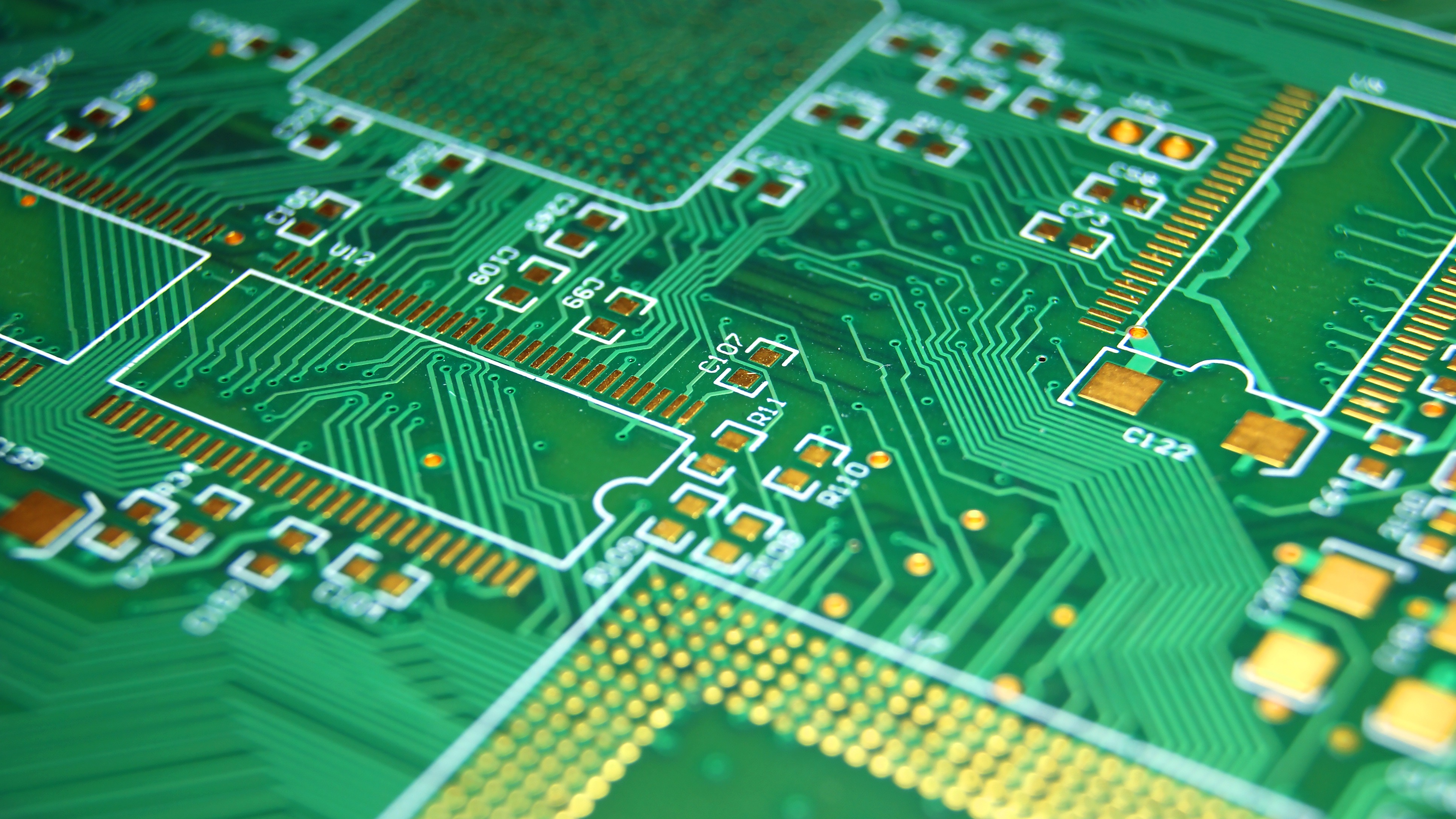
What Are the Signal Integrity and Manufacturing Implications?
Copper weight also impacts signal integrity, especially in high-speed and RF circuits where controlled impedance is critical. Beyond performance, manufacturing considerations and costs are significant.
Signal Integrity and Impedance Control
● 1oz Copper: Its thinner profile makes 1oz copper well-suited for high-density designs featuring fine traces (e.g., 4-6 mils wide). It allows for tighter spacing and is easier to etch, making it ideal for complex, high-speed digital circuits, such as DDR memory interfaces operating at 1-3 GHz. To achieve a 50-ohm characteristic impedance, a 1oz copper trace on a standard 1.6mm FR-4 board typically requires a width of about 10-12 mils, which is generally manageable in most layouts.
● 2oz Copper: The thicker 2oz copper demands wider traces to achieve the same impedance, as impedance decreases with increasing conductor thickness. For a 50-ohm trace, a 2oz copper trace might need to be 15-18 mils wide, which can complicate routing in densely packed designs. However, 2oz copper's lower resistance reduces signal attenuation, thereby improving performance in high-frequency AC signals, such as RF circuits operating at 5-10 GHz.
Engineers designing high-speed circuits should utilize simulation tools (e.g., Altium Designer or Cadence) to accurately model impedance and verify trace geometries, especially when opting for 2oz copper.
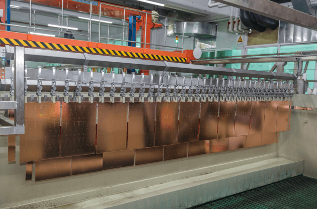
Manufacturing Considerations and Costs
While 2oz copper offers superior electrical and thermal performance, it presents specific manufacturing challenges and typically incurs higher costs.
● Etching: The thicker 2oz copper requires extended etching times, which can result in undercutting and less precise trace geometries. This increases the minimum trace width and spacing requirements (e.g., 6-8 mils for 2oz versus 4-5 mils for 1oz), thereby limiting design flexibility in high-density boards.
● Lamination: The added thickness of 2oz copper can lead to uneven pressure during the lamination process, potentially causing board warping or delamination. Manufacturers must employ balanced stackups (e.g., matching copper weights on opposing layers) to mitigate these issues.
● Cost: Using 2oz copper generally increases material costs by 20-50% compared to 1oz copper, depending on the board's size and layer count. The increased complexity in fabrication also contributes to higher production costs, particularly for multilayer boards.
1oz copper, being the industry standard, is generally more cost-effective and easier to manufacture. Most PCB fabricators default to 1oz copper unless otherwise specified, which simplifies production for standard designs.
How Can Current-Carrying Capacity Be Optimized in PCB Designs?
To maximize current-carrying capacity without exclusively relying on thicker copper, engineers can implement several effective design strategies.
Practical Design Strategies
● Widen Traces: The simplest method to boost current capacity is to increase trace width. For example, doubling the width of a 1oz copper trace from 10 mils to 20 mils can increase its current capacity from 1A to approximately 1.8A (with a 10°C rise).
● Utilize Multiple Layers: Distributing current across parallel traces or planes on different layers helps reduce resistance and heat accumulation. For instance, connecting two 1oz copper planes with vias can achieve performance comparable to a single 2oz plane.
● Enhance with Solder Mask and Paste: For 1oz copper traces nearing their thermal limits, removing the solder mask and applying solder paste during reflow can effectively increase the cross-sectional area, boosting current capacity by 10-20%.
● Incorporate Copper Bus Bars: In extreme high-current applications (e.g., above 100A), soldering dedicated copper bus bars onto PCB pads can manage currents that standard traces cannot handle.
● Improve Cooling: Enhancing airflow with fans or integrating heat sinks can allow 1oz copper to manage higher currents by reducing the operating temperature rise.
These techniques often make 1oz copper sufficient for many applications, reserving 2oz copper for scenarios where space or thermal constraints are particularly demanding.
Related Reading: How to Avoid Common PCB Design Mistakes with 1 oz Copper
When Should Engineers Choose 1oz Versus 2oz Copper?
The decision between 1oz and 2oz copper hinges on your project's specific electrical, thermal, and budgetary requirements.
When to Select 1oz Copper
● For applications with low to moderate currents (typically below 5A).
● For high-density designs that require fine traces and tight spacing.
● For cost-sensitive projects where sufficient board space allows for wider traces.
● For standard digital or low-power analog circuits.
When to Select 2oz Copper
● For high-current applications (exceeding 5A) or power electronics.
● For designs requiring superior thermal management or operation in high-temperature environments.
● For circuits where board space is constrained, making wider traces impractical.
● For applications demanding high reliability, such as automotive or aerospace systems.
For designs that fall into a borderline category, consider performing a power delivery network (PDN) analysis using specialized tools like Saturn PCB Toolkit to quantify voltage drops and temperature rises. It is generally recommended to include a 10-20% safety margin above calculated current requirements to account for environmental variations and potential design tolerances.
Partnering with AIVON for Your PCB Copper Weight Needs
At AIVON, we recognize the critical importance of selecting the correct copper weight to ensure your PCB's performance and reliability. Our advanced manufacturing capabilities support both 1oz and 2oz copper designs, employing precise etching and lamination processes to deliver high-quality results. Whether you require quick-turn prototyping to validate your high-current design or comprehensive global logistics for large-scale production, we provide end-to-end solutions tailored to meet engineers' diverse needs. Our team also conducts design-for-manufacturability (DFM) reviews to optimize your stackup and trace geometries, helping you achieve the ideal balance of performance and cost.
Concluding Thoughts on Copper Weight Selection
The choice between 1oz and 2oz copper is a pivotal decision in PCB design, directly influencing current-carrying capacity, thermal management, signal integrity, and overall cost. While 1oz copper is often the preferred option for most standard applications, offering a cost-effective and versatile solution for low-to-moderate power circuits, 2oz copper excels in high-power and high-reliability designs where space and thermal constraints are paramount.


