Introduction
FR-4, a widely used material in printed circuit board (PCB) fabrication, serves as the backbone for countless electronic devices due to its cost-effectiveness and reliable performance. A critical aspect of PCB design involves vias, which are conductive pathways connecting different layers of a board. Understanding FR-4 PCB via types, their design rules, and manufacturing considerations is essential for electrical engineers aiming to optimize signal integrity and ensure manufacturability. Vias, including microvias and buried vias, play a pivotal role in high-density interconnects and multilayer designs. This article explores the various FR-4 PCB via types, outlines key design rules like aspect ratio constraints, and addresses manufacturing challenges to guide engineers in creating robust and efficient PCB layouts.
What Are FR-4 PCB Vias and Why Do They Matter?
Vias in FR-4 PCB are small holes drilled or laser-etched into the board, filled or plated with conductive material, to establish electrical connections between layers. FR-4, a flame-retardant epoxy laminate, is the standard substrate for most PCBs due to its mechanical strength and thermal stability. Vias are vital for routing signals and power in multilayer designs, especially as electronic devices shrink and demand higher component density.
Without properly designed vias, signal loss, crosstalk, or manufacturing defects can compromise a PCB's performance. FR-4 PCB via types, such as through-hole, blind, buried, and microvias, each serve specific purposes based on design needs. For instance, microvias enable finer routing in high-density interconnect (HDI) boards, while buried vias save surface space. Understanding their roles and limitations ensures reliable electrical performance and cost-effective production.
Types of FR-4 PCB Vias
Through-Hole Vias
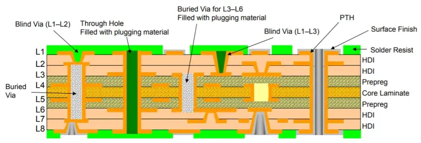
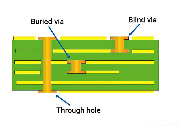
Through-hole vias extend from the top to the bottom layer of a PCB, passing through all layers. They are the simplest and most common type in FR-4 designs, often used for mounting components or connecting power and ground planes. These vias are mechanically drilled, making them cost-effective but space-intensive, as they occupy all layers.
Blind Vias
Blind vias connect an outer layer to an inner layer without passing through the entire board. They are ideal for HDI designs in FR-4 PCBs, as they free up space on the opposite side. Typically formed by controlled-depth drilling or laser processes, blind vias support denser layouts but increase manufacturing complexity.
Buried Vias
FR-4 PCB buried vias connect internal layers without reaching the outer surfaces. Hidden within the board, they maximize surface area for components and reduce signal interference. Buried vias are common in multilayer FR-4 designs but require precise layer alignment during fabrication, adding to circuit board cost.
Microvias
FR-4 PCB microvias are small-diameter vias, often less than 0.15 mm, used in HDI applications. Created via laser drilling, they connect adjacent layers and support fine-pitch components. Microvias are critical for compact designs but demand strict control over FR-4 PCB via aspect ratio to ensure plating uniformity and reliability.
FR-4 PCB Via Design Rules for Electrical Engineers
Designing vias for FR-4 PCBs requires adherence to specific guidelines to balance performance and manufacturability. These rules address via size, spacing, aspect ratio, and placement, ensuring signal integrity and structural stability.
Via Size and Aspect Ratio
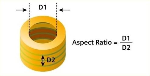
FR-4 PCB via aspect ratio, defined as the ratio of via depth to diameter, is a critical parameter. A high aspect ratio can lead to plating issues, risking open circuits. Industry standards, such as IPC-6012E, recommend maintaining an aspect ratio below 10:1 for through-hole vias and 1:1 for microvias to ensure reliable copper deposition during fabrication.
Via Spacing and Placement
Spacing between vias must prevent electrical shorts and mechanical stress. Vias placed too closely can weaken the FR-4 substrate, causing cracks. Guidelines from IPC-A-600K suggest a minimum spacing of 0.2 mm for microvias and 0.5 mm for larger vias, depending on board thickness and layer count. Placement near high-speed signal traces should also minimize interference.
Pad and Annular Ring Design
The pad surrounding a via, along with its annular ring, must provide sufficient area for soldering or plating. A minimum annular ring width, as per IPC-6012E, ensures mechanical stability. For FR-4 PCB via design rules, a ring width of at least 0.1 mm for inner layers and 0.15 mm for outer layers is often advised.
Thermal and Electrical Considerations
Vias in FR-4 PCBs must handle thermal expansion and electrical loads. Large current-carrying vias may require multiple smaller vias to distribute heat and current evenly. Signal integrity in high-frequency designs also demands controlled impedance, which can be affected by via stub length. Trimming stubs or using back-drilling aligns with best practices under IPC standards.
Manufacturing Considerations for FR-4 PCB Vias
Fabricating vias in FR-4 PCBs involves multiple processes, each with unique challenges. Engineers must consider these factors to avoid defects and ensure consistent quality during production.
Drilling and Plating Challenges
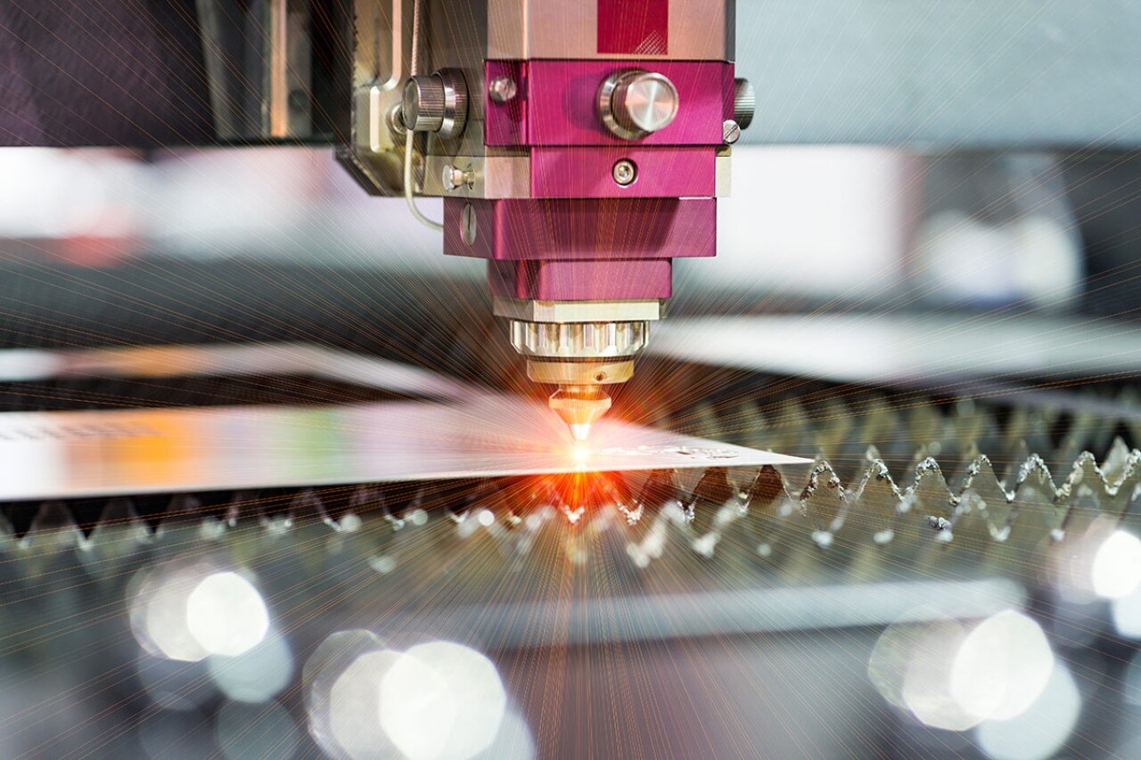
Mechanical drilling, used for through-hole and some blind vias, can cause burrs or misalignment in FR-4 material if not controlled. Laser drilling, essential for FR-4 PCB microvias, offers precision but requires careful calibration to avoid damaging the epoxy laminate. Plating uniformity is another concern, especially with high FR-4 PCB via aspect ratio designs, as uneven copper deposition leads to weak connections.
Layer Alignment for Buried Vias
FR-4 PCB buried vias demand precise layer registration during lamination. Misalignment can result in open circuits or shorts, as specified in IPC-A-600K for acceptability criteria. Sequential lamination processes, often used for buried vias, increase production time and cost but are necessary for complex multilayer boards.
Thermal Stress and Reliability
FR-4 material has a defined glass transition temperature, typically around 130 to 140 degrees Celsius, beyond which it may deform. Vias must withstand thermal cycles during soldering or operation without cracking. IPC-6012E outlines test methods for thermal stress, recommending via designs that minimize stress concentration points.
Cost Implications
Complex via structures like FR-4 PCB microvias and buried vias raise manufacturing costs due to specialized equipment and additional process steps. Engineers must weigh performance benefits against budget constraints, often opting for simpler through-hole vias in less demanding applications to maintain cost efficiency.
Best Practices for Optimizing FR-4 PCB Via Design
To achieve reliable and manufacturable FR-4 PCB designs, engineers can follow these actionable best practices rooted in industry standards.
- Limit via aspect ratios to recommended values per IPC-6012E to ensure plating quality.
- Use microvias sparingly in HDI designs, focusing on adjacent layer connections to reduce complexity.
- Incorporate sufficient spacing between vias, adhering to IPC-A-600K guidelines, to avoid structural issues.
- Simulate thermal and electrical performance during design to predict via behavior under load.
- Collaborate with fabrication teams early to align design rules with manufacturing capabilities.
Troubleshooting Common Via Issues in FR-4 PCBs
Issues with vias often arise during design or manufacturing, impacting PCB performance. Identifying and resolving these problems is crucial for engineers.
Plating Voids
Plating voids occur when copper fails to deposit uniformly inside vias, often due to high FR-4 PCB via aspect ratio or contamination. Inspection per IPC-A-600K can detect voids, while redesigning with lower aspect ratios or improved cleaning processes prevents recurrence.
Via Cracking
Cracking in vias results from thermal or mechanical stress, especially in FR-4 material subjected to temperature cycles. Following IPC-6012E thermal stress test guidelines helps identify weak points. Adding support structures or reducing via density near stress areas mitigates this issue.
Signal Integrity Loss
High-speed designs may suffer from signal loss due to via stubs or improper impedance matching. Back-drilling to remove stubs or using simulation tools to optimize via placement ensures better performance, aligning with industry best practices.
Conclusion
Vias are indispensable in FR-4 PCB designs, enabling multilayer connectivity and supporting compact, high-performance electronics. By understanding FR-4 PCB via types such as through-hole, blind, buried, and microvias, engineers can select the appropriate structure for their application. Adhering to FR-4 PCB via design rules, including aspect ratio limits and spacing guidelines, ensures signal integrity and manufacturability. Manufacturing considerations, from drilling precision to thermal stress management, further influence via reliability. Implementing best practices and troubleshooting common issues equips electrical engineers to create robust FR-4 PCB layouts that meet stringent industry standards and project requirements.
FAQs
Q1: What are the main FR-4 PCB via types used in multilayer designs?
A1: FR-4 PCB via types include through-hole vias, which span all layers, blind vias connecting outer to inner layers, buried vias linking internal layers, and microvias for high-density interconnects. Each type serves specific purposes based on space and performance needs. Understanding their applications helps engineers optimize layouts for signal integrity and component density in multilayer FR-4 designs.
Q2: How does FR-4 PCB via aspect ratio affect manufacturing reliability?
A2: FR-4 PCB via aspect ratio, the depth-to-diameter ratio, impacts plating quality during manufacturing. High ratios can cause uneven copper deposition, leading to weak connections. Standards like IPC-6012E suggest keeping ratios below 10:1 for through-hole vias and 1:1 for microvias. Maintaining these limits ensures reliable electrical performance and reduces the risk of defects in FR-4 PCBs.
Q3: What design rules should be followed for FR-4 PCB microvias?
A3: For FR-4 PCB microvias, design rules focus on small diameters, typically under 0.15 mm, and low aspect ratios around 1:1 per IPC-6012E. Adequate spacing, often 0.2 mm minimum as per IPC-A-600K, prevents structural issues. Placement should avoid high-stress areas, and laser drilling precision must be ensured to maintain reliability in high-density FR-4 designs.
Q4: Why are FR-4 PCB buried vias important for compact layouts?
A4: FR-4 PCB buried vias connect internal layers without reaching outer surfaces, freeing up space for components and reducing signal interference. They are crucial for compact multilayer layouts where surface area is limited. Although they increase manufacturing complexity due to alignment needs per IPC-A-600K, their ability to optimize space makes them valuable in dense FR-4 PCB designs.
References
IPC-6012E - Qualification and Performance Specification for Rigid Printed Boards. IPC, 2020.
IPC-A-600K - Acceptability of Printed Boards. IPC, 2020.