Introduction
Metal Core Printed Circuit Boards, often referred to as MCPCBs, play a vital role in applications requiring superior thermal management. These boards are essential in industries like LED lighting, power electronics, and automotive systems where heat dissipation is critical. Unlike traditional FR4 boards, MCPCBs use a metal substrate, typically aluminum or copper, to enhance thermal conductivity. This guide provides a detailed look into the MCPCB manufacturing process, from initial design to final assembly. Aimed at electrical engineers, this article explores key steps in metal core PCB manufacturing, focusing on fabrication techniques and assembly processes. Understanding these stages ensures optimal performance and reliability in high heat environments. Let's dive into the intricate world of insulated metal substrate technology and its production workflow.
What Is MCPCB and Why It Matters
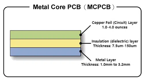
MCPCB stands for Metal Core Printed Circuit Board, a specialized type of PCB designed to manage heat effectively. It consists of a metal base layer, a dielectric layer for insulation, and a copper circuit layer on top. The metal core, often aluminum or copper, acts as a heat sink, drawing thermal energy away from critical components. This structure is particularly beneficial in applications with high power density, where overheating can lead to failure.
The importance of MCPCB fabrication lies in its ability to extend the lifespan of electronic devices. Efficient heat dissipation reduces thermal stress on components, improving reliability. For electrical engineers, selecting MCPCBs over standard boards can be a game changer in designs for LED arrays, motor controllers, and power converters. With rising demands for compact, high performance electronics, understanding metal core PCB manufacturing becomes essential for innovative solutions.
Technical Principles of MCPCB Fabrication
MCPCB fabrication differs from traditional PCB production due to the integration of a metal substrate. The core principle is to balance thermal conductivity with electrical insulation. The metal base provides a pathway for heat to escape, while the dielectric layer prevents short circuits between the metal and copper traces. This dual functionality requires precise material selection and process control.
The dielectric layer in an insulated metal substrate is typically a thin, thermally conductive material. It must withstand high temperatures and provide adequate insulation. The copper layer, bonded to the dielectric, forms the circuit pattern through etching processes. Engineers must consider thermal expansion coefficients of all layers to prevent delamination during operation. Standards like IPC-6012E guide the qualification and performance of such boards, ensuring structural integrity.
Another key aspect is surface finish compatibility with the metal core. Finishes like ENIG or HASL must adhere well to copper without compromising the thermal path. Fabrication challenges include maintaining flatness and avoiding warpage, which can affect assembly. Adhering to industry standards ensures that MCPCB manufacturing steps address these technical demands effectively.
Step-by-Step MCPCB Manufacturing Process
Step 1: Design and Material Selection
The journey of metal core PCB manufacturing begins with design. Engineers use software to create layouts, defining circuit patterns and thermal vias. Material selection is crucial, as the metal core type, dielectric thickness, and copper weight impact performance. Aluminum is often chosen for its cost effectiveness and thermal properties, while copper offers superior conductivity for demanding applications.
Step 2: Metal Core Preparation
Once materials are selected, the metal core is cut to size and cleaned to remove contaminants. Surface treatment ensures proper adhesion of the dielectric layer. Precision in this step is vital to avoid defects that could disrupt later stages of MCPCB fabrication.
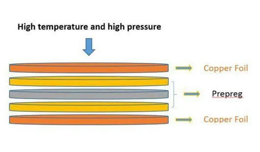
Step 3: Dielectric Layer Application
The dielectric layer, an insulated metal substrate component, is applied to the metal core. This layer is laminated under controlled heat and pressure to bond securely. Uniform thickness is critical to maintain consistent thermal and electrical properties across the board.
Step 4: Copper Foil Lamination
A thin copper foil is laminated onto the dielectric layer. This process requires precise alignment to ensure the circuit pattern will be accurate. The bond strength between layers is tested against standards like IPC-A-600K to confirm acceptability.
Step 5: Circuit Pattern Imaging and Etching
The copper layer is coated with a photoresist material, and the circuit design is transferred using photolithography. Unwanted copper is etched away, leaving the desired traces. This step in MCPCB manufacturing steps demands accuracy to prevent shorts or open circuits.
Step 6: Drilling and Routing
Holes for vias and mounting are drilled into the board. Routing shapes the board to its final dimensions. For MCPCBs, drilling must account for the metal core's hardness, requiring specialized tools to avoid damage.
Step 7: Surface Finish Application
A surface finish is applied to protect copper traces and ensure solderability. Common finishes comply with standards like JEDEC J-STD-020E for moisture and reflow sensitivity. This step enhances the board's durability during the MCPCB assembly process.
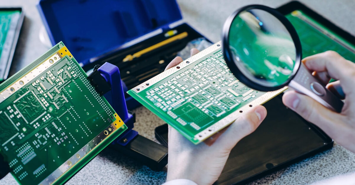
Step 8: Quality Inspection
Before moving to assembly, boards undergo rigorous inspection. Tests for dimensional accuracy, layer adhesion, and thermal conductivity are conducted. Standards such as IPC-A-600K provide guidelines for acceptability, ensuring only quality boards proceed.
MCPCB Assembly Process: From Components to Final Product
Component Placement Planning
The MCPCB assembly process starts with planning component placement. Engineers prioritize thermal management, placing heat generating components near thermal vias or directly above the metal core. Layouts are optimized to minimize heat buildup and ensure efficient dissipation.
Solder Paste Application
Solder paste is applied to pads using a stencil, aligning with the circuit design. Precision in this step prevents bridging or insufficient solder during reflow. The paste must meet thermal requirements of MCPCB applications, often guided by industry standards.
Component Mounting
Components are mounted onto the board using automated pick and place machines. Accuracy ensures proper alignment with solder paste deposits. For MCPCBs, care is taken to avoid stress on the board, which could cause warpage due to the metal substrate.
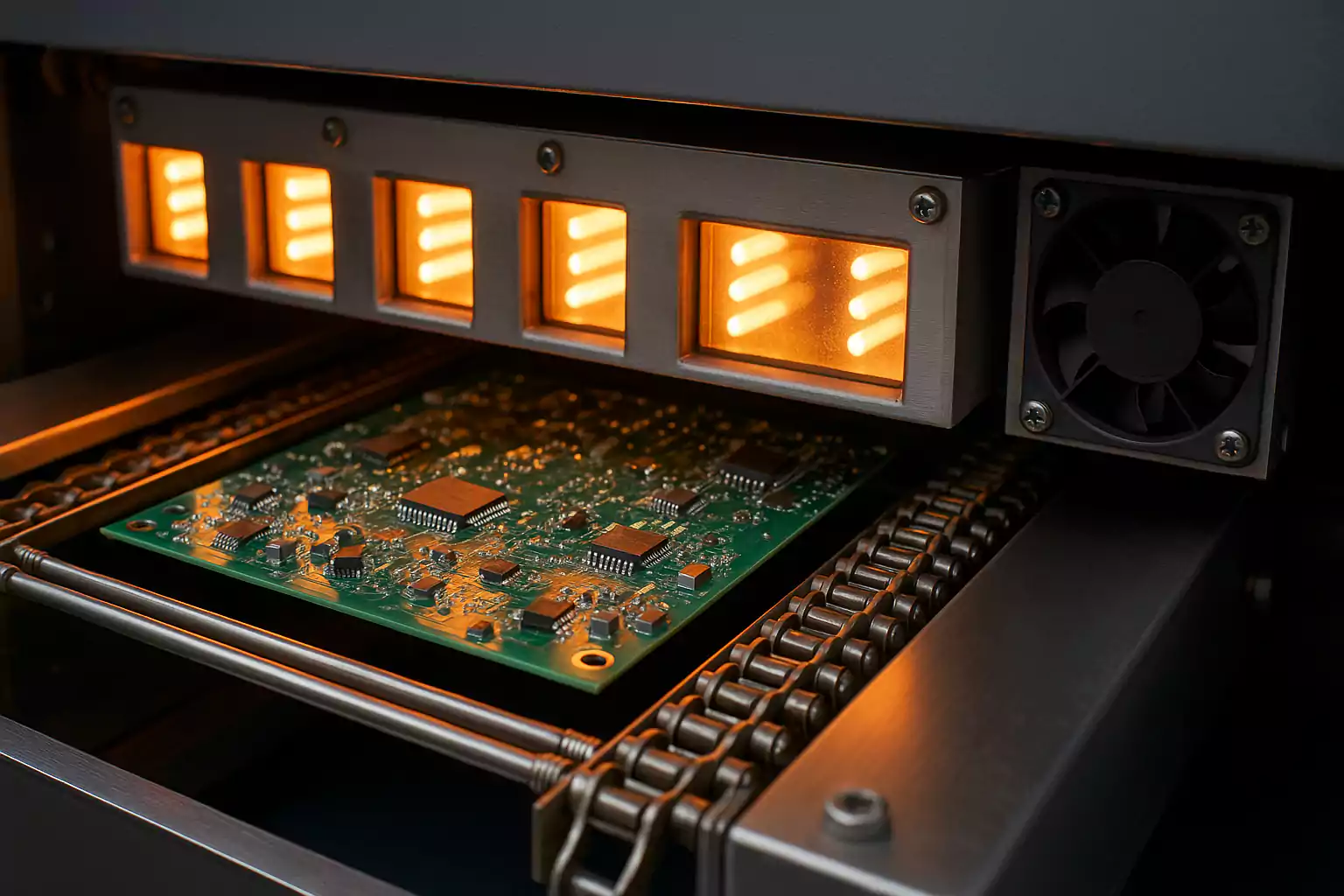
Reflow Soldering
Boards pass through a reflow oven, where solder paste melts and forms connections. Temperature profiles are tailored to MCPCB materials, preventing damage to the dielectric layer. Adherence to JEDEC J-STD-020E ensures components withstand the process without degradation.
Final Inspection and Testing
Post assembly, boards are inspected for solder joint quality and component alignment. Electrical testing verifies functionality, while thermal imaging may assess heat dissipation. Standards like IPC-6012E provide performance benchmarks for reliability.
Best Practices for MCPCB Design and Manufacturing
To achieve optimal results in metal core PCB manufacturing, engineers should focus on material compatibility. Matching thermal expansion rates between layers reduces stress during temperature changes. Incorporating thermal vias near high power components enhances heat transfer to the metal core.
During MCPCB fabrication, maintaining cleanliness prevents defects in lamination. Controlling lamination pressure and temperature ensures uniform bonding. Engineers must also verify drilling parameters to avoid damaging the metal substrate, which can compromise structural integrity.
In the MCPCB assembly process, customizing reflow profiles to board specifications minimizes thermal shock. Regular calibration of equipment sustains precision in component placement and soldering. Following standards like ISO 9001:2015 for quality management supports consistent outcomes across production batches.
Challenges in MCPCB Manufacturing and Solutions
One challenge in MCPCB manufacturing steps is managing warpage due to the differing properties of metal and dielectric materials. This can be mitigated by selecting balanced stackups and adhering to design guidelines in IPC-6012E. Another issue is dielectric breakdown under high voltage, which requires thorough testing of insulated metal substrate layers.
Drilling through metal cores poses difficulties due to hardness. Using carbide tools and optimized feed rates prevents tool wear and board damage. Additionally, ensuring adhesion between layers demands strict process control, aligning with IPC-A-600K acceptability criteria to avoid delamination.
Conclusion
The MCPCB manufacturing process is a complex yet rewarding journey from design to assembly. Each step, from material selection to final testing, plays a crucial role in delivering boards with exceptional thermal performance. For electrical engineers, mastering metal core PCB manufacturing and assembly processes unlocks potential in high power applications. By adhering to industry standards and best practices, reliable and efficient MCPCBs can be produced consistently. This guide serves as a foundation for understanding and optimizing the fabrication of insulated metal substrates for advanced electronics.
FAQs
Q1: What are the key steps in the MCPCB fabrication process?
A1: The MCPCB fabrication process includes design, material selection, metal core preparation, dielectric application, copper lamination, circuit imaging, etching, drilling, surface finishing, and quality inspection. Each step ensures thermal efficiency and electrical insulation. Precision in lamination and etching is vital to meet standards like IPC-6012E for performance and reliability in high heat applications.
Q2: How does the MCPCB assembly process differ from standard PCB assembly?
A2: The MCPCB assembly process focuses on thermal management, requiring tailored reflow profiles to protect the metal core and dielectric layer. Component placement prioritizes heat dissipation, often near thermal vias. Standards like JEDEC J-STD-020E guide soldering to prevent thermal damage, unlike standard PCB assembly where heat is less critical.
Q3: Why is insulated metal substrate important in MCPCB manufacturing?
A3: Insulated metal substrate is crucial in MCPCB manufacturing as it provides electrical insulation between the metal core and copper traces while conducting heat. This dielectric layer ensures safety and performance in high power applications. Its quality directly impacts thermal efficiency and reliability, aligning with standards like IPC-A-600K for acceptability.
Q4: What challenges arise during metal core PCB manufacturing?
A4: Challenges in metal core PCB manufacturing include warpage from material mismatch, dielectric breakdown, and drilling difficulties due to metal hardness. Solutions involve balanced stackups, rigorous testing per IPC-6012E, and using specialized tools. Process control during lamination prevents delamination, ensuring consistent quality across production.
References
IPC-6012E — Qualification and Performance Specification for Rigid Printed Boards. IPC, 2020.
IPC-A-600K — Acceptability of Printed Boards. IPC, 2020.
JEDEC J-STD-020E — Moisture/Reflow Sensitivity Classification. JEDEC, 2014.
ISO 9001:2015 — Quality Management Systems. ISO, 2015.