Introduction
Component placement in printed circuit board design plays a critical role in ensuring smooth transitions from prototyping to high-volume production. Engineers often focus on electrical performance during initial layout, but overlooking manufacturing and assembly implications can lead to costly rework, delays, and yield losses. Optimizing placement early incorporates design for manufacturability principles, aligning component positioning with automated processes like pick-and-place and reflow soldering. This approach minimizes defects such as misalignment, solder bridging, and thermal stress failures. For electric engineers, mastering PCB assembly component placement means balancing functionality, reliability, and producibility from the start.
What Is Component Placement Design for Manufacturability and Why It Matters
Component placement design for manufacturability, often called DFM component placement, refers to strategically positioning electronic parts on a PCB to facilitate fabrication and assembly while maintaining performance. It involves considerations like accessibility for machines, solder joint integrity, and mechanical stability. Poor placement can cause issues like component shadowing during reflow or excessive board warpage under thermal cycling. In contrast, well-optimized layouts reduce assembly time, lower defect rates, and improve overall yield. Industry standards such as IPC-2221C outline general placement requirements to guide designers toward reliable outcomes. Ultimately, effective DFM component placement ensures designs scale efficiently from low-mix prototypes to mass production.
This practice matters because modern electronics demand denser boards with mixed surface-mount and through-hole components. Assembly lines rely on high-speed robots that require precise fiducials and consistent orientations for accuracy. Misplaced tall components can interfere with stencil printing or vacuum nozzles, leading to troubleshooting headaches. By prioritizing manufacturability, engineers avoid common pitfalls that inflate costs by forcing manual interventions or scrap. The payoff appears in faster time-to-market and higher first-pass yields, critical for competitive projects.
Technical Principles of PCB Assembly Component Placement
Several engineering principles govern PCB assembly component placement, starting with mechanical balance to prevent warpage. Heavy or tall components placed near edges create uneven stress during reflow, causing the board to bow and misalign subsequent parts. Distributing mass symmetrically across the board maintains flatness, especially for multilayer stacks with varying copper densities. Thermal expansion differences between components and the substrate further influence placement, as mismatched coefficients lead to solder joint fatigue over time.
Assembly processes impose additional constraints, particularly for surface-mount technology. Pick-and-place machines achieve micron-level accuracy but falter with obstructed paths or non-standard orientations. Components must allow clear access for nozzles, avoiding overlaps that block vision systems. Solder paste deposition via stencils requires adequate spacing to prevent bridging between adjacent pads. Reflow soldering dynamics, including surface tension and gravity, pull components into alignment, but excessive distances can cause tombstoning in small passives.
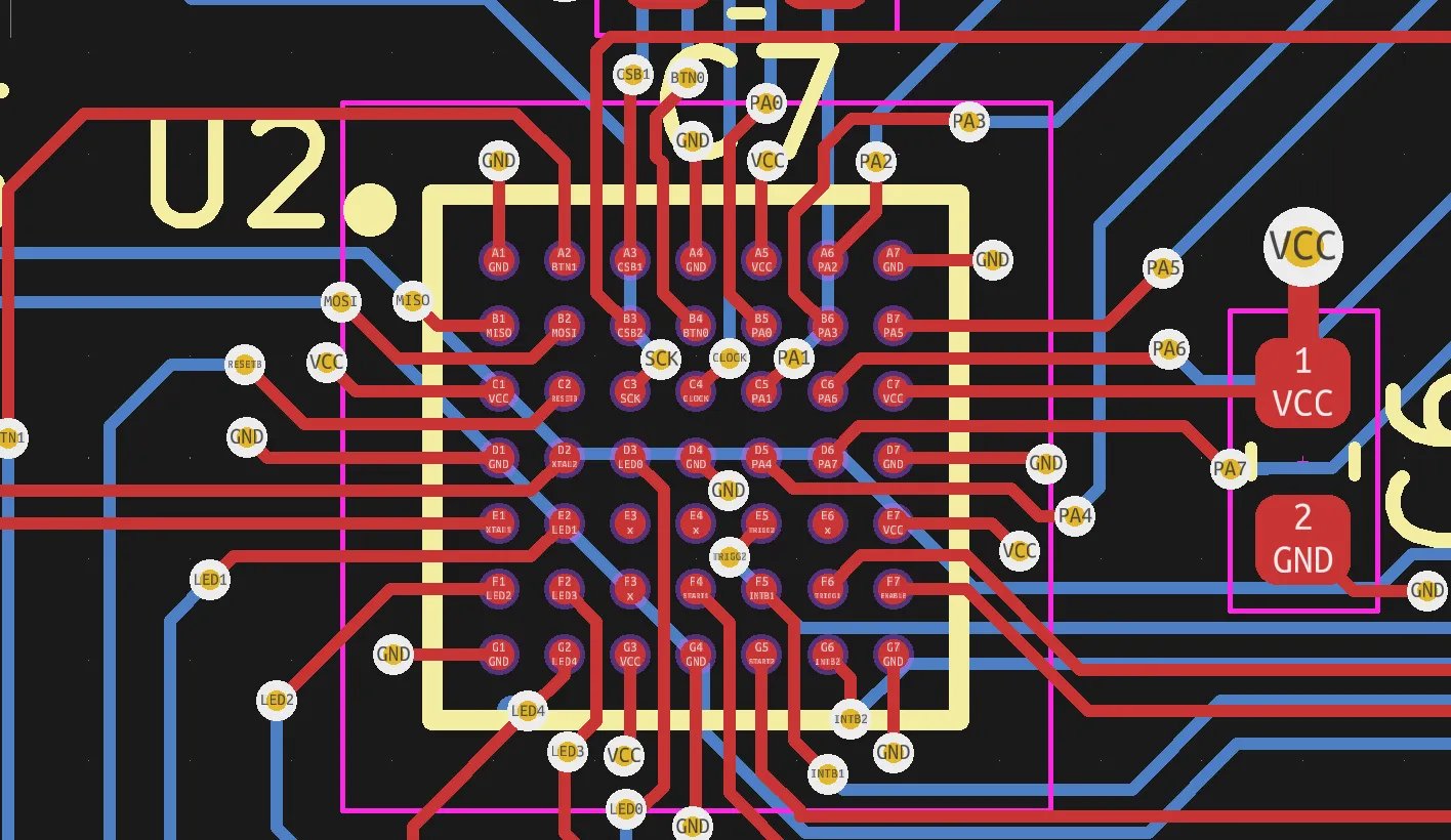
IPC-7351C provides guidelines for land patterns that support precise placement by defining pad geometries optimized for solder volume and self-alignment. Signal integrity principles also factor in, as high-speed signals benefit from short, grouped traces between related parts. Power and ground planes demand decoupling capacitors placed close to IC pins to minimize inductance. These interconnected factors ensure the layout supports both electrical function and assembly robustness.
Practical Best Practices for DFM Component Placement
Start with functional grouping to streamline PCB assembly component placement. Cluster analog, digital, and power sections separately to isolate noise and simplify routing. Orient all polar capacitors and resistors in the same direction, reducing machine head changes and speeding up placement. This uniformity aids troubleshooting, as consistent alignments make visual inspections faster during quality control.
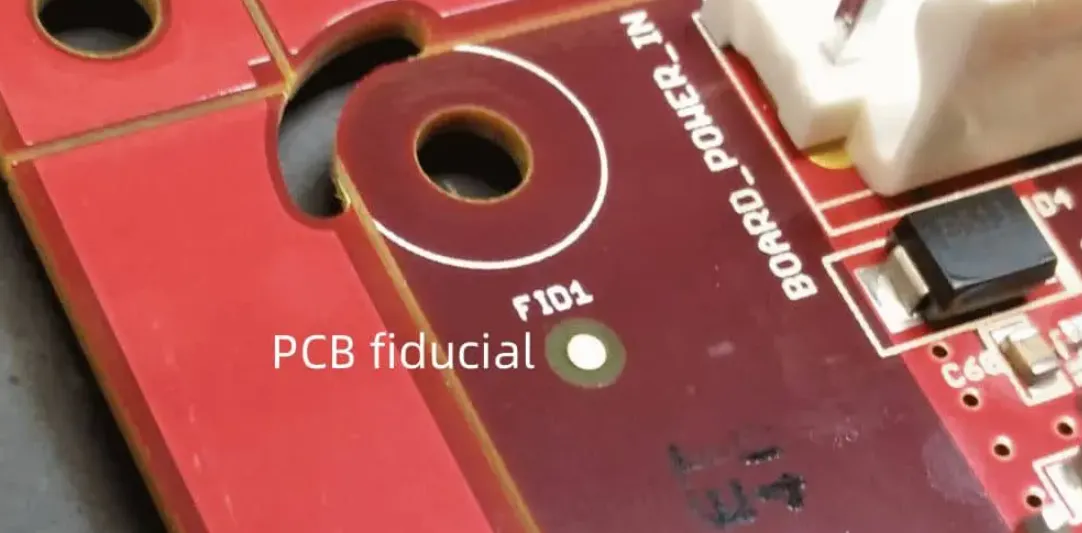
Maintain generous clearances around board edges, typically beyond connector pins or mounting holes, to accommodate clamping fixtures and depaneling tools. Place fiducial marks in all four corners and near dense areas, sized appropriately for camera recognition without interfering with traces. For mixed-technology boards, position through-hole components on the top side to avoid bottom-side obstructions during wave soldering. Surface-mount devices dominate the top layer, with bottom-side placement reserved for low-profile parts to prevent damage from handling.
Address thermal management by locating heat-generating ICs centrally or near heat sinks, with bypass capacitors within millimeters of power pins. Avoid shadowing by staggering rows of components under taller ones, ensuring even reflow heating. Simulate placement for warpage using finite element analysis if possible, adjusting heavy parts like transformers inward. Adhering to IPC-A-610J criteria during design previews helps predict acceptable solder joints post-assembly.
Incorporate design rule checks for minimum pitch between parts, scaling with component size to match pick-and-place tolerances. Test panels with multiple identical boards include shared fiducials for batch efficiency. Document placement rationale in assembly notes, specifying no-go zones for adhesives or conformal coatings. These steps form a robust DFM component placement strategy, minimizing iterations between design and fabrication.
Troubleshooting Common Placement Issues
Engineers frequently encounter misalignment from inadequate fiducials or board flex during handling. Verify fiducial contrast against copper planes and ensure they exceed machine vision thresholds. Warpage often stems from asymmetric placement; counter it by mirroring heavy components across the centerline. Tombstoning in chip resistors signals uneven paste or preheat issues, resolved by refining land patterns per IPC-7351C.
Solder bridging arises in tight pitches; increase spacing or use finer stencil apertures. For double-sided assemblies, sequence bottom-side tall parts first to avoid top-side interference. Post-reflow inspections per IPC-A-610J reveal placement offsets, prompting gerber adjustments. Systematic reviews of assembly feedback loops refine future designs, turning issues into proactive guidelines.
Conclusion
Optimizing component placement bridges the gap between innovative PCB design and reliable production. By embracing component placement design for manufacturability from schematic capture, engineers sidestep assembly bottlenecks and enhance product longevity. Key practices like grouping, orientation, and balance, guided by standards, deliver manufacturable layouts. Troubleshooting empowers iterative improvements, ensuring consistent quality. Prioritizing these elements positions teams for efficient, defect-free manufacturing.
FAQs
Q1: What is component placement design for manufacturability?
A1: Component placement design for manufacturability integrates assembly process constraints into PCB layout to boost yield and reduce costs. It focuses on spacing, orientation, and balance to suit pick-and-place machines and reflow ovens. Standards like IPC-2221C provide foundational rules for clearances and fiducials. Practical steps include grouping functions and avoiding edge placements. This proactive approach prevents common defects like bridging or warpage.
Q2: How does PCB assembly component placement impact yield?
A2: PCB assembly component placement directly affects yield by influencing solder joint quality and machine efficiency. Poor orientation increases pick errors, while unbalanced mass causes warpage and misalignment. Optimal layouts with fiducials and standard pitches enable high-speed automation. Troubleshooting offsets via IPC-A-610J inspections refines processes. Engineers see yield gains through fewer rework cycles and faster throughput.
Q3: What are key DFM component placement guidelines for mixed boards?
A3: DFM component placement for mixed through-hole and SMT boards prioritizes top-side through-hole positioning to clear wave soldering paths. Stagger SMT parts to prevent reflow shadowing, and center heavy components for stability. Use IPC-7351C land patterns for reliable self-alignment. Maintain edge clearances for fixturing. These guidelines minimize handling damage and assembly defects.
Q4: Why group components in PCB assembly component placement?
A4: Grouping components in PCB assembly component placement shortens traces, isolates noise, and eases machine programming. Analog signals stay away from digital clocks, reducing EMI risks. Uniform orientations cut placement time by avoiding rotations. This strategy aligns with DFM principles, improving inspectability per IPC-A-610J. Resulting boards assemble faster with higher first-pass success.
References
IPC-2221C — Generic Standard on Printed Board Design. IPC, 2023
IPC/J-STD-001J — Requirements for Soldered Electrical and Electronic Assemblies. IPC, 2024
IPC-A-610J — Acceptability of Electronic Assemblies. IPC, 2024
IPC-7351C — Generic Requirements for Surface Mount Design and Land Pattern Standard. IPC, 2018