Introduction
Surface Mount Technology (SMT) soldering is a cornerstone of modern electronics assembly, enabling the production of compact and high-performance devices. However, defects in SMT soldering can lead to costly rework, reduced reliability, and product failures. For electrical engineers, understanding how to prevent these issues is critical to ensuring quality and efficiency. This article focuses on practical strategies to avoid common SMT soldering defects, with an emphasis on soldering paste selection, solder paste application techniques, pad and pin maintenance practices, and the nuances of lead-free soldering. By addressing these areas, engineers can enhance assembly outcomes and meet stringent industry standards. Whether working on prototype designs or high-volume production, the tips provided here aim to support robust and reliable soldering processes.
Why SMT Soldering Defects Matter
SMT soldering defects are a significant concern in electronics manufacturing due to their impact on product performance and production costs. Issues such as insufficient solder, bridging, tombstoning, and cold joints can compromise electrical connections, leading to device malfunctions or complete failures. These defects often stem from improper solder paste application, degraded pads or pins, or challenges associated with lead-free soldering materials. For electrical engineers, minimizing these problems is essential to maintain high yield rates and ensure compliance with quality standards like those outlined in IPC specifications. Addressing defects proactively also reduces rework expenses and enhances customer satisfaction by delivering reliable products.
Technical Causes of SMT Soldering Defects
Understanding the root causes of SMT soldering defects is the first step in prevention. Several factors contribute to these issues during the assembly process.
Solder Paste Related Problems
Soldering paste, a critical material in SMT PCB assembly, consists of flux and metal alloy particles. Its quality and composition directly influence soldering outcomes. Poor storage conditions, such as exposure to high temperatures or humidity, can degrade the paste, leading to issues like insufficient wetting or void formation. Incorrect viscosity or particle size distribution may also cause uneven deposition during solder paste application, resulting in defects like bridging or insufficient solder. Standards such as IPC J-STD-005A provide guidelines for solder paste requirements and testing to ensure consistency and performance.
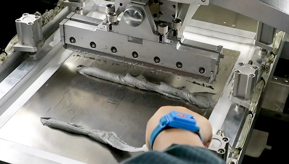
Issues in Solder Paste Application
The method of solder paste application significantly affects soldering quality. Stencil printing, a common technique, requires precise control over parameters like stencil thickness, aperture design, and printing pressure. Misalignment or excessive pressure can lead to smearing or insufficient paste on pads, causing open joints or tombstoning. Additionally, inadequate cleaning of stencils between runs can introduce contaminants, further compromising the process. Adhering to best practices outlined in IPC-7525B for stencil design and application helps mitigate these risks.
Pad and Pin Maintenance Challenges
Degraded or contaminated pads and pins are frequent culprits behind soldering defects. Oxidation on copper pads or component leads prevents proper wetting, leading to weak or incomplete joints. Physical damage to pads, such as scratches or delamination, can also disrupt solder flow. For lead-free soldering, higher reflow temperatures exacerbate these issues by accelerating oxidation if surfaces are not properly maintained. Regular inspection and cleaning, as recommended by IPC-A-600K, are vital to ensure surface integrity.
Lead-Free Soldering Complications
Lead-free soldering, driven by environmental regulations, introduces unique challenges due to the higher melting points of alloys like SAC (tin-silver-copper). These elevated temperatures, often around 217 to 221 degrees Celsius as per JEDEC J-STD-020E, increase thermal stress on components and boards, potentially causing warpage or cracking. Additionally, lead-free alloys exhibit poorer wetting characteristics compared to traditional tin-lead solders, heightening the risk of cold joints or insufficient solder. Engineers must adapt reflow profiles and material selections to address these properties.
Practical Solutions to Prevent SMT Soldering Defects
Implementing effective strategies can significantly reduce the occurrence of SMT soldering defects. Below are actionable tips tailored for electrical engineers focusing on key areas of concern.
Optimizing Soldering Paste Selection and Storage
Choosing the right soldering paste is crucial for reliable SMT assembly. Engineers should select pastes that comply with IPC J-STD-005A, ensuring appropriate flux activity and alloy composition for the specific application. For lead-free soldering, SAC305 is a widely used alloy due to its balance of mechanical strength and thermal performance. Store solder paste in controlled environments, typically between 2 to 10 degrees Celsius, to prevent degradation. Always check expiration dates and avoid reusing paste that has been exposed to air for extended periods.
Mastering Solder Paste Application Techniques
Precision in solder paste application starts with proper stencil design and setup. Use stencils with aperture sizes and shapes that match component pad dimensions, following guidelines in IPC-7525B. Maintain consistent printing parameters, such as squeegee speed and pressure, to achieve uniform paste deposition. Regularly inspect and clean stencils with appropriate solvents to remove residue. Employing automated optical inspection systems post-printing can help detect application errors early, ensuring defects are addressed before reflow.

Ensuring Pad and Pin Maintenance
Effective pad and pin maintenance begins with routine cleaning to remove oxidation and contaminants. Use isopropyl alcohol and lint-free wipes for manual cleaning, or ultrasonic methods for larger batches, as suggested by IPC-A-600K for surface preparation. Protect pads from physical damage during handling by using anti-static mats and tools. For lead-free soldering, consider applying a thin layer of flux prior to assembly to enhance wetting on oxidized surfaces. Regularly inspect pads and pins under magnification to identify issues like delamination or cracks.

Adapting to Lead-Free Soldering Requirements
Lead-free soldering demands careful adjustment of reflow profiles to accommodate higher melting temperatures. Follow JEDEC J-STD-020E for moisture sensitivity and reflow guidelines to prevent thermal damage. Use nitrogen atmospheres during reflow if possible, as this reduces oxidation at elevated temperatures. Select components and boards with finishes like ENIG (Electroless Nickel Immersion Gold) that are compatible with lead-free alloys for better wetting. Monitor peak temperatures and time above liquidus to ensure proper joint formation without overheating.
Suggested Reading: SMT Testing in SMT PCB Assembly Process
Troubleshooting Common SMT Soldering Defects
Electrical engineers often encounter recurring defects in SMT assembly. Here are practical approaches to diagnose and resolve these issues based on hands-on experience.
Addressing Bridging and Insufficient Solder
Bridging occurs when excess solder connects adjacent pads, often due to over-application of soldering paste. Inspect stencil apertures for oversized openings and adjust printing parameters. Insufficient solder, conversely, results from inadequate paste volume or poor wetting. Verify paste viscosity and stencil alignment, and ensure pads are free of oxidation per IPC-A-600K standards. Adjusting reflow profiles to optimize wetting time can also help.
Mitigating Tombstoning and Cold Joints
Tombstoning, where components stand upright due to uneven solder melting, can be minimized by balancing pad sizes and ensuring uniform heating. Cold joints, characterized by dull or cracked appearances, often stem from inadequate heat or flux activity, especially in lead-free soldering. Extend preheat stages in the reflow profile as per JEDEC J-STD-020E to ensure thorough activation of flux and complete melting of solder.
Conclusion
Preventing SMT soldering defects requires a comprehensive approach that addresses soldering paste quality, precise solder paste application, diligent pad and pin maintenance, and tailored strategies for lead-free soldering. By adhering to industry standards like IPC and JEDEC guidelines, electrical engineers can mitigate common issues such as bridging, tombstoning, and cold joints. Implementing the practical tips outlined in this article ensures higher assembly yields and reliable electronic products. Continuous monitoring and process optimization remain essential to adapt to evolving materials and technologies in SMT manufacturing.
FAQs
Q1: How does soldering paste quality affect SMT assembly outcomes?
A1: Soldering paste quality is vital for reliable SMT assembly. Poor paste can lead to defects like insufficient wetting or voiding, impacting joint strength. Selecting pastes that meet IPC J-STD-005A standards ensures consistent performance. Proper storage and handling also prevent degradation, maintaining viscosity and flux activity for optimal results during application.
Q2: What are best practices for solder paste application in SMT?
A2: Effective solder paste application relies on precise stencil design and controlled printing parameters. Follow IPC-7525B guidelines for aperture sizing and stencil thickness. Maintain consistent squeegee pressure and speed for uniform deposition. Regular stencil cleaning and post-printing inspection help catch errors early, ensuring defect-free soldering in SMT processes.
Q3: Why is pad and pin maintenance crucial for soldering success?
A3: Pad and pin maintenance prevents defects by ensuring clean, oxide-free surfaces for soldering. Contaminated or damaged pads hinder wetting, leading to weak joints. Regular cleaning, as per IPC-A-600K, and protective handling reduce risks. This is especially critical in lead-free soldering where higher temperatures worsen oxidation issues.
Q4: What challenges does lead-free soldering present in SMT?
A4: Lead-free soldering involves higher melting points, increasing thermal stress on components and boards. Per JEDEC J-STD-020E, this can cause warpage or cracking if not managed. Poor wetting of lead-free alloys also risks cold joints. Adjusting reflow profiles and using compatible finishes like ENIG are essential to overcome these challenges.
References
IPC J-STD-005A — Requirements for Soldering Pastes. IPC, 2012.
IPC-7525B — Stencil Design Guidelines. IPC, 2011.
IPC-A-600K — Acceptability of Printed Boards. IPC, 2020.
JEDEC J-STD-020E — Moisture/Reflow Sensitivity Classification for Nonhermetic Surface Mount Devices. JEDEC, 2014.


