Introduction
In the intricate world of electronics manufacturing, ensuring the quality and reliability of printed circuit boards (PCBs) remains a critical priority for electrical engineers. PCB inspection methods play a vital role in identifying defects, preventing failures, and maintaining compliance with industry standards. With various technologies available, such as automated optical inspection (AOI), X-ray inspection, and flying probe testing equipment, selecting the right approach can be challenging. Each method offers unique strengths for defect analysis in PCBs and caters to different production needs. This guide provides a detailed PCB inspection methods comparison, focusing on AOI versus X-ray inspection, alongside flying probe testing, to help engineers make informed decisions. By understanding the capabilities and limitations of these automated inspection systems, professionals can optimize quality control processes and ensure high performance in their designs.
Why PCB Inspection Matters
PCBs serve as the backbone of electronic devices, connecting components and enabling functionality. Even minor defects, such as misaligned components, solder issues, or hidden cracks, can lead to catastrophic failures in critical applications. Effective inspection identifies these issues early, reducing rework costs and ensuring reliability. For electrical engineers, choosing the appropriate inspection method is not just about meeting standards like IPC-A-600K but also about safeguarding product integrity. Whether using AOI for surface-level checks, X-ray for internal defect analysis in types of PCBs, or flying probe testing for prototype validation, each technique addresses specific challenges. The stakes are high in industries like aerospace, medical, and automotive, where quality directly impacts safety. Thus, understanding these automated inspection systems is essential for maintaining excellence in manufacturing and design workflows.
Technical Principles of PCB Inspection Methods
Automated Optical Inspection (AOI)
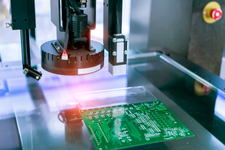
AOI systems utilize high-resolution cameras and advanced imaging software to inspect PCBs for surface-level defects. This method captures detailed images of the board, comparing them against a predefined template or design file to detect issues like missing components, incorrect placements, and solder defects. AOI operates on the principle of light reflection and pattern recognition, often employing multiple light sources to highlight anomalies. It excels in high-volume production environments due to its speed and non-contact nature. However, AOI is limited to visible defects and cannot inspect hidden solder joints or internal layers. Its effectiveness depends on proper lighting and camera angles, making it ideal for post-assembly checks in surface-mount technology processes.
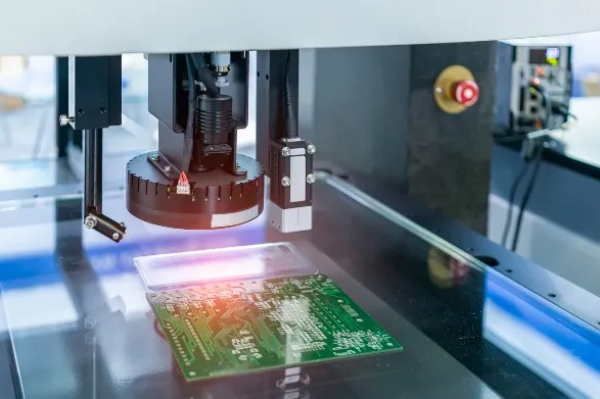
Suggested Reading: PCB Prototyping Assembly: Ensuring Quality with Automated Optical Inspection (AOI)
X-Ray Inspection
X-ray inspection, often referred to as automated X-ray inspection (AXI), penetrates the PCB to reveal internal structures invisible to optical methods. This technique uses X-ray radiation to create detailed images of solder joints, vias, and internal layers, making it indispensable for defect analysis in PCBs with complex designs like ball grid arrays (BGAs). It can detect voids, insufficient solder, and misalignments beneath components. The principle relies on the differential absorption of X-rays by materials of varying densities, allowing precise imaging. While highly effective for hidden defects, X-ray inspection is slower and more costly than AOI. It also requires trained personnel to interpret images and ensure compliance with safety regulations due to radiation exposure risks.
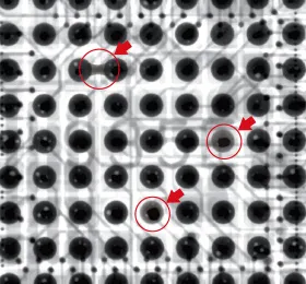
Suggested Reading: Mastering PCB X-ray Inspection: A Beginner's Step-by-Step Guide
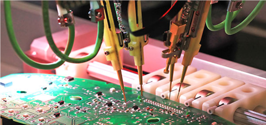
Flying Probe Testing Equipment
Flying probe testing employs movable probes to perform electrical testing on PCBs without the need for custom fixtures. This method measures resistance, capacitance, and continuity by contacting test points on the board, identifying issues like open circuits and shorts. Unlike traditional in-circuit testing (ICT), which requires dedicated test fixtures, flying probe systems offer flexibility, making them suitable for low-volume production and prototypes. The principle involves precise robotic control of probes to access densely populated boards. While effective for electrical defect analysis in PCBs, this method is slower than AOI and X-ray for large-scale production. Its non-destructive nature and adaptability, however, make it a valuable tool for early-stage validation.
Comparing AOI, X-Ray, and Flying Probe Testing
To assist electrical engineers in selecting the right inspection method, a PCB inspection methods comparison is essential. Each technology addresses specific defect types and production scenarios. Below is a structured overview of their capabilities, limitations, and ideal applications.
-
Automated Optical Inspection (AOI)
- Primary Use: Surface-level defect detection
- Defects Detected: Missing components, misplacement, solder issues
- Advantages: Fast, cost-effective, non-contact
- Limitations: Cannot inspect hidden defects
- Best Suited For: High-volume production, SMT lines
-
X-Ray Inspection (AXI)
- Primary Use: Internal and hidden defect analysis
- Defects Detected: Solder voids, BGA issues, internal cracks
- Advantages: Detects hidden defects, high precision
- Limitations: Slow, expensive, safety concerns
- Best Suited For: Complex boards, BGAs, quality audits
-
Flying Probe Testing
- Primary Use: Electrical functionality testing
- Defects Detected: Open circuits, shorts, continuity issues
- Advantages: Flexible, no fixtures needed
- Limitations: Slow for high volume, limited to electrical tests
- Best Suited For: Prototypes, low-volume runs
This comparison highlights that AOI versus X-ray inspection often depends on whether surface or internal defects are the priority. AOI excels in speed for visible issues, while X-ray is unmatched for hidden flaws. Flying probe testing equipment, meanwhile, fills the gap for electrical validation, especially in smaller batches where fixture costs are prohibitive.
Practical Guidance for Selecting Inspection Equipment
Assessing Production Volume and Budget
When choosing between automated inspection systems, production volume and budget are key factors. For high-volume manufacturing, AOI systems provide rapid throughput at a lower cost per board, aligning with the need for efficiency. In contrast, X-ray inspection suits quality-critical applications where internal defect analysis in PCBs justifies the higher investment. Flying probe testing equipment is ideal for low-volume or prototype stages, as it avoids the expense of custom fixtures required by traditional ICT setups. Engineers should evaluate long-term costs, including maintenance and training, alongside initial equipment prices to ensure alignment with project goals.
Matching Inspection to Defect Types
Understanding the specific defects likely in a PCB design guides method selection. If surface defects like component misalignment dominate, AOI offers sufficient coverage. For multilayer boards or packages with hidden solder joints, X-ray inspection becomes essential. When electrical integrity is the concern, such as in early design validation, flying probe testing equipment provides direct feedback on connectivity. Combining methods, such as using AOI for initial screening and X-ray for detailed checks, often yields the best results, especially in compliance with standards like IPC-6012E for rigid board performance.
Considering Board Complexity and Design
PCB complexity influences the choice of inspection technology. Simple, single-layer boards may only require AOI for quick visual checks. Complex designs with dense component placement or multiple layers demand X-ray for internal defect analysis in PCBs. Flying probe testing suits boards with accessibility challenges, as probes can target specific points without fixture constraints. Engineers must review design files and assembly processes to anticipate inspection needs, ensuring the selected method matches the board’s technical requirements.
Integration into Manufacturing Workflow
Seamless integration of automated inspection systems into existing workflows enhances efficiency. AOI systems fit well post-reflow in surface-mount lines, providing immediate feedback. X-ray inspection often serves as a secondary check for critical assemblies, placed after initial screening. Flying probe testing equipment works best in prototype labs or small-batch setups, offering flexibility without disrupting larger production lines. Coordination with manufacturing teams ensures inspection stages align with assembly steps, minimizing bottlenecks and maintaining quality per IPC-A-600K acceptability criteria.
Troubleshooting Common Inspection Challenges
Electrical engineers often face challenges in PCB inspection, such as false positives in AOI due to lighting variations or difficulty interpreting X-ray images for subtle defects. To address AOI inaccuracies, regular calibration and template updates are necessary to match design specifications. For X-ray systems, training on image analysis helps distinguish actual defects from artifacts, ensuring precise defect analysis in PCBs. Flying probe testing may encounter issues with probe alignment on dense boards, requiring careful programming of test points. Documenting recurring issues and adjusting inspection parameters based on standards like IPC-6012E can mitigate these problems, improving overall reliability.
Conclusion
Selecting the right PCB inspection equipment is a strategic decision for electrical engineers aiming to ensure quality and reliability in electronics manufacturing. This guide on PCB inspection methods comparison highlights the strengths of AOI, X-ray inspection, and flying probe testing equipment. AOI offers speed for surface defects, X-ray excels in internal defect analysis in PCBs, and flying probe testing provides flexibility for electrical validation. By assessing production needs, defect types, and board complexity, engineers can integrate these automated inspection systems effectively. Aligning choices with industry standards ensures compliance and performance, ultimately enhancing product integrity in demanding applications.
FAQs
Q1: What are the key differences in AOI versus X-ray inspection for PCB quality control?
A1: AOI focuses on surface defects like component misalignment using cameras, offering speed for high-volume production. X-ray inspection penetrates boards to detect hidden issues such as solder voids in BGAs, ensuring thorough defect analysis in PCBs. While AOI is cost-effective and fast, it misses internal flaws. X-ray, though slower and pricier, is vital for complex designs requiring deep inspection.
Q2: How does flying probe testing equipment support prototype development?
A2: Flying probe testing equipment is ideal for prototypes due to its flexibility and fixtureless design. It performs electrical tests for continuity and shorts by accessing specific points on the PCB. This method suits low-volume runs, allowing engineers to validate designs without costly setups. It ensures early detection of electrical issues, streamlining the development process.
Q3: Which automated inspection systems are best for high-volume PCB manufacturing?
A3: For high-volume PCB manufacturing, automated optical inspection (AOI) systems stand out due to their speed and cost efficiency. They quickly identify surface defects post-assembly, fitting seamlessly into fast-paced production lines. While X-ray can be used selectively for critical checks, AOI remains the primary choice for maintaining throughput without compromising basic quality control.
Q4: How can defect analysis in PCBs be improved with combined inspection methods?
A4: Combining inspection methods enhances defect analysis in PCBs by addressing diverse flaw types. AOI can screen for surface issues initially, followed by X-ray inspection for hidden defects like internal solder problems. Flying probe testing adds electrical verification. This layered approach, aligned with industry standards, ensures comprehensive coverage, reducing the risk of undetected faults in critical applications.
References
IPC-A-600K — Acceptability of Printed Boards. IPC, 2020.
IPC-6012E — Qualification and Performance Specification for Rigid Printed Boards. IPC, 2020.